
Production method for polysilicon grid of DRAM

A technology of polysilicon gate and manufacturing method, which is applied in semiconductor/solid-state device manufacturing, electrical components, semiconductor devices, etc., can solve problems such as word line and bit line short circuit, and achieve the effect of solving short circuit and solving prominent problems

Inactive Publication Date: 2008-10-29
SEMICON MFG INT (SHANGHAI) CORP +1
View PDF0 Cites 6 Cited by
  • Summary
  • Abstract
  • Description
  • Claims
  • Application Information

AI Technical Summary

Problems solved by technology

[0007] The purpose of the present invention is to provide an improved method for making polysilicon gates in DRAMs, so as to solve the problem of short circuit between word lines and bit lines caused by tungsten silicide protrusion that usually occurs

Method used


Image

  • Production method for polysilicon grid of DRAM
  • Production method for polysilicon grid of DRAM
  • Production method for polysilicon grid of DRAM

Examples


Embodiment 1

[0048] Figure 3a~3c It is a schematic diagram of the fabrication process of the polysilicon gate according to an embodiment of the present invention. Wherein, firstly, the gate silicon oxide layer 22 is formed by thermally growing silicon oxide on the silicon substrate, with a thickness of 4.0-8.0 nanometers. The thermally grown silicon oxide used is a conventional method and will not be described in detail here.

[0049] Then, the polysilicon layer 23 is deposited and formed by using conventional techniques, such as chemical vapor deposition, with a thickness of 60-100 nm.

[0050] Forming the tungsten silicide (WSix) layer 24 on the polysilicon layer can adopt conventional techniques, such as on the polysilicon layer, first depositing tungsten with chemical vapor deposition, and then heating to make tungsten and polysilicon at high temperature, such as 565 ℃, under pressure Under 1.2 Torr, react for 45 seconds to form tungsten silicide with a thickness of 80-120 nm.

[0...

Embodiment 2

[0059] Figures 4a-4e It is a schematic diagram of the fabrication process of the polysilicon gate according to another embodiment of the present invention.

[0060] Wherein, firstly, the gate silicon oxide layer 22 is formed by thermally growing silicon oxide on the silicon substrate, with a thickness of 4.0-8.0 nanometers. The thermally grown silicon oxide used is a conventional method and will not be described in detail here.

[0061] Then, the polysilicon layer 23 is deposited and formed by using conventional techniques, such as chemical vapor deposition, with a thickness of 60-100 nanometers.

[0062] To form the WSix layer 24 on the polysilicon layer, conventional techniques can be used, such as first depositing tungsten on the polysilicon layer by chemical vapor deposition, and then heating to make the tungsten and polysilicon react at a high temperature, such as 565° C. and a pressure of 1.2 Torr, for 45 seconds. , forming tungsten silicide, the thickness of which is...


PUM

PropertyMeasurementUnit
depthaaaaaaaaaa
thicknessaaaaaaaaaa
thicknessaaaaaaaaaa

Abstract

The invention relates to a manufacture method for a polysilicon grid in a dynamic random memorizer (DRAM); the method includes the following steps of: forming a monox layer, a polysilicon layer, a tungsten silicide layer and a silicon nitride layer sequentially on an underlay; etching the silicon nitride layer; etching a part of the tungsten silicide layer by wetting; etching the tungsten silicide layer; etching the polysilicon layer and etching the monox layer. The method can solve the problem of short circuit (flip bit line) between a word line and a bit line existing during the manufacture process of the polysilicon grid of the prior art and avoid short circuit from being generated between the word line and the bit line of the DRAM.

Description

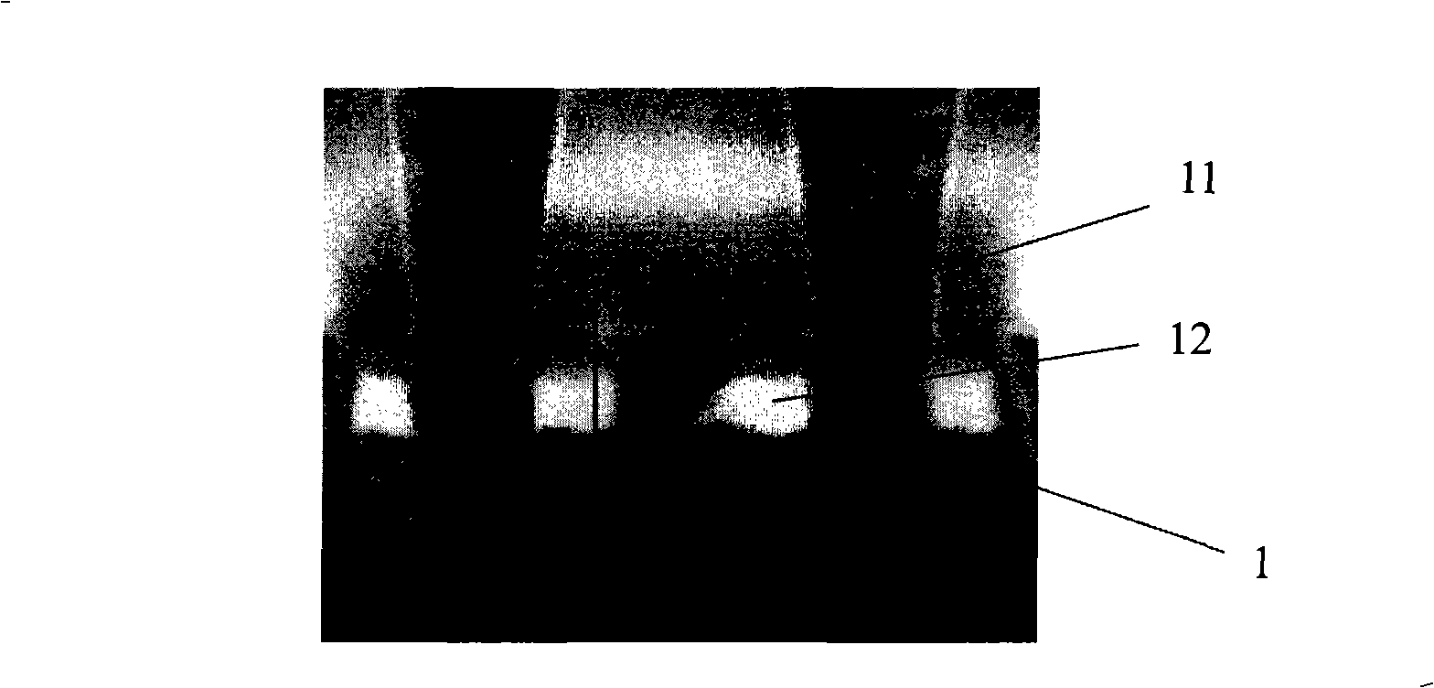
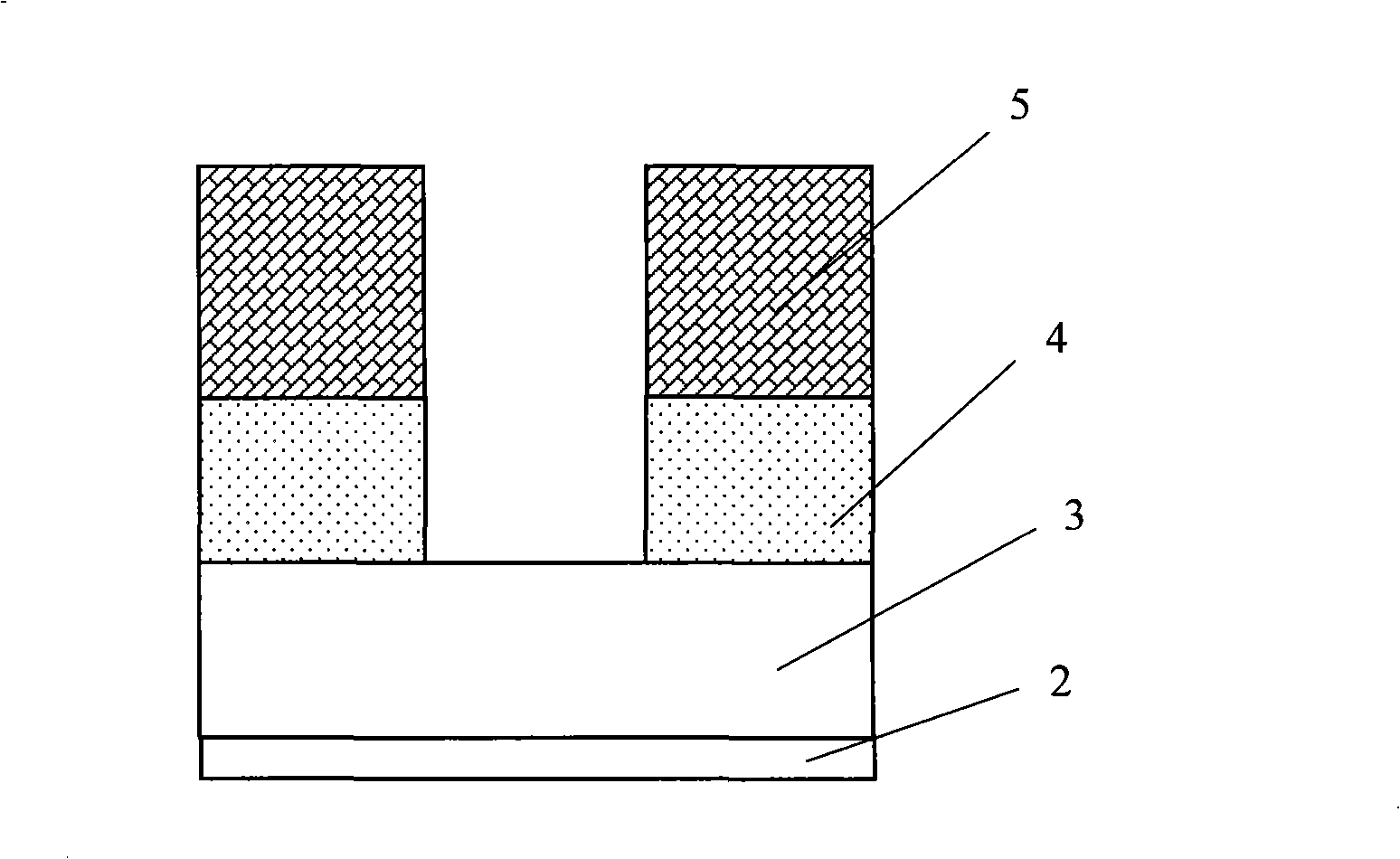
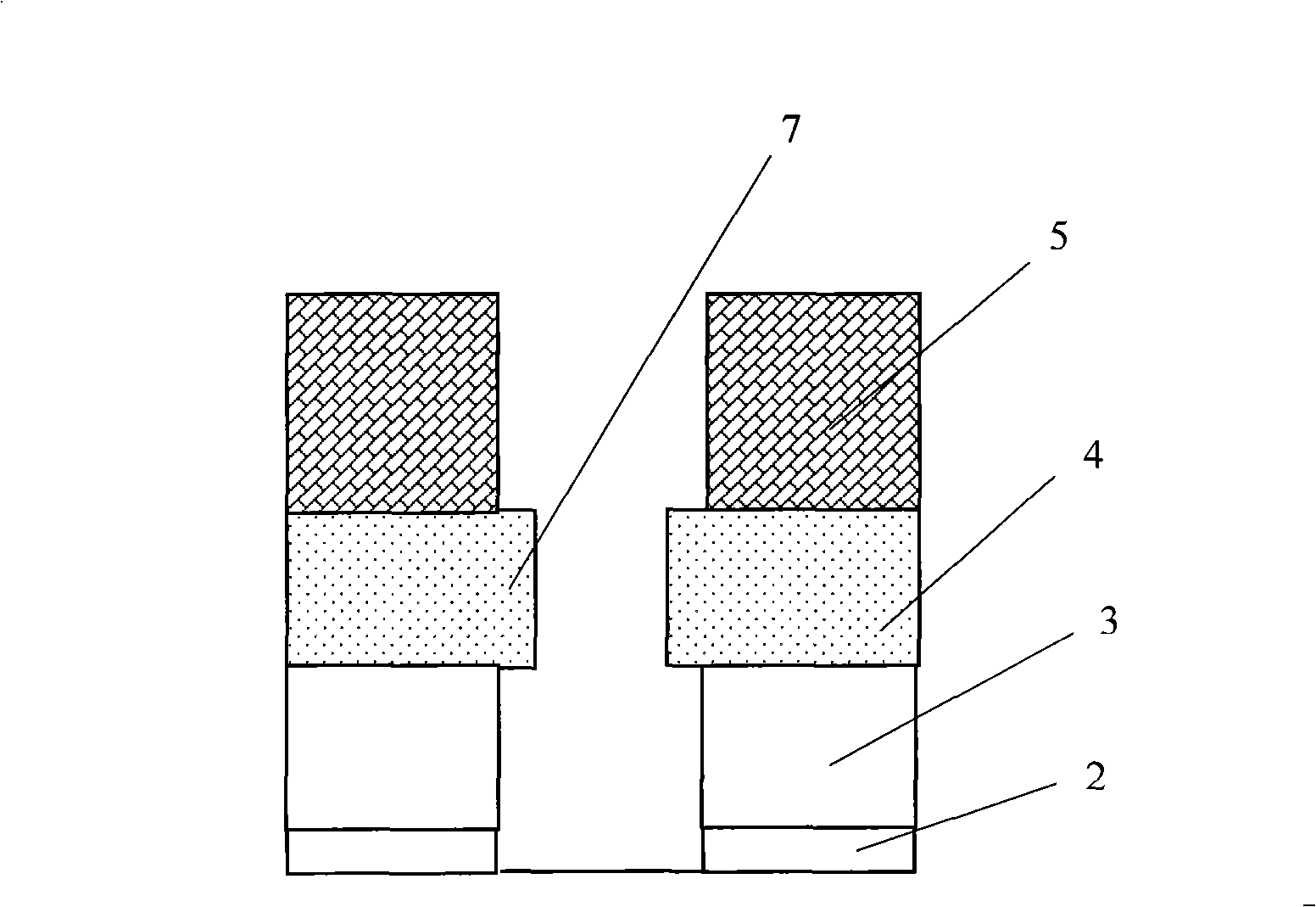
technical field [0001] The invention relates to a manufacturing process of a semiconductor device, in particular to a manufacturing method of a polysilicon gate for solving the problem of short circuit (flip bit line) between a word line and a bit line during the manufacturing process of a dynamic random access memory (DRAM). Background technique [0002] The previous DRAM had the problem of flip bit line between the word line and the bit line, which was caused by the tungsten silicide (WSix) protrusion of the polysilicon gate (P1L) after the thermal cycle process, such as figure 1 shown. The problem generation process is described below. [0003] figure 1 Electron microscope photo of the polysilicon gate cross-section at the end of the process (End of line, EOL) of the sample that has the problem of short circuit (flip bit line) between the word line and the bit line. . Figure 2a-2e is a schematic diagram of the generation process of the short circuit (flip bit line) p...

Claims


Application Information

Patent Timeline
Patent Type & Authority Applications(China)
IPC IPC(8): H01L21/28H01L21/336H01L21/8242H10B12/00
Inventor 代培刚
Owner SEMICON MFG INT (SHANGHAI) CORP
Learn More