Method for enhancing pattern uniformity

A uniformity and pattern technology, applied in the field of semiconductor structure manufacturing, can solve the problems of poor pattern uniformity, unresolvable pattern size difference, lower component operation efficiency and electrical performance, etc., to improve pattern uniformity and reduce size poor effect

Active Publication Date: 2010-05-26
MACRONIX INT CO LTD
View PDF4 Cites 0 Cited by
  • Summary
  • Abstract
  • Description
  • Claims
  • Application Information

AI Technical Summary

Problems solved by technology

However, this method only shrinks the patterned photoresist layer on the memory cell area and the semi-open area of ​​the pattern, but the difference in the size of the pattern on the memory cell area and the semi-open area of ​​the pattern is still unresolved.
As a result of poor pattern uniformity, the conductive wires formed on the semi-empty area of ​​the pattern will still be larger than the conductive wires on the memory cell area, which cannot meet the electrical requirements of the device, and reduce the operating efficiency and electrical performance of the device.

Method used


Image

  • Method for enhancing pattern uniformity
  • Method for enhancing pattern uniformity
  • Method for enhancing pattern uniformity

Examples


Embodiment Construction

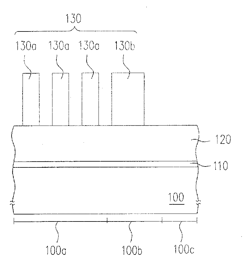
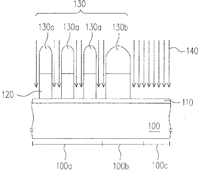
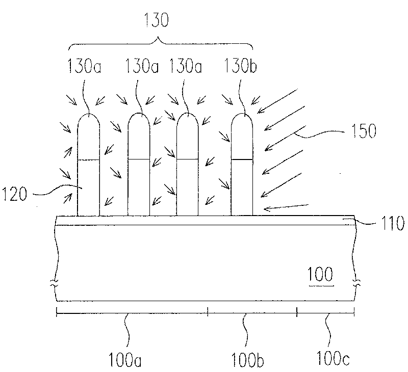
[0027] Figure 1A to Figure 1C is a cross-sectional flow diagram illustrating a method for improving pattern uniformity according to an embodiment of the present invention.

[0028] see Figure 1A , this method is applicable to the substrate 100, and the substrate 100 includes a pattern dense area 100a, a pattern semi-empty area 100b and a pattern empty area 100c. Wherein, the pattern semi-empty area 100b refers to the boundary area between the pattern dense area 100a and the pattern empty area 100c. In one embodiment, the substrate 100 may be a semiconductor wafer, the pattern dense area 100a is, for example, a memory cell area, the pattern empty area 100c is, for example, a logic element area, and the pattern semi-empty area 100b is, for example, a memory cell area and a logic element area the middle area. Wherein, for example, memory cells have been formed on the pattern dense area 100 a , and general logic elements have been formed on the pattern empty area 100 c , for e...


PUM


Abstract

The invention relates to a method for enhancing pattern uniformity, suitable for a substrate comprising a pattern concentration region and a pattern quasi-vacant region. The substrate is sequentiallyformed with a barrier layer and a bottom antireflective layer. The method comprises: first forming a patterned photo-resistant layer; the patterned photo-resistant layer comprises a first photo-resistant pattern in the pattern concentration region, and a second photo-resistant pattern in the pattern quasi-vacant region, wherein the size of the second photo-resistant pattern is larger than the sizeof the first photo-resistant pattern; then carrying the first clipping step to realize micro-patterned process on the photo-resistant layer, meanwhile, removing part of the bottom antireflective layer by using the patterned photo-resistant layer as a covering shield; then carrying out the second clipping step to realize micro-pattern process on the photo-resistant layer and the bottom antireflective layer simultaneously, and minimizing the size differences between the second photo-resistant pattern and the first photo-resistant pattern. The invention can be used for enhancing the pattern uniformity.

Description

technical field [0001] The invention relates to a method for manufacturing a semiconductor structure, in particular to a method for improving pattern uniformity. Background technique [0002] With the rapid development of the field of integrated circuits, high performance, high integration, low cost, light weight and small size have become the goals pursued by the design and manufacture of electronic products. For the current semiconductor industry, in order to meet the above goals, it is often necessary to manufacture components with multiple functions on the same chip, for example, combining read-only memory, static random access memory, flash memory or dynamic random access memory. Access memory, logic circuits, digital circuits, etc. are fabricated on the same chip, which is the so-called System On Chip (SOC). [0003] However, the traditional system-on-chip (SOC) integrates various components on the same chip, which can improve its functionality and electrical function...

Claims


Application Information

Patent Timeline
Patent Type & Authority Patents(China)
IPC IPC(8): H01L21/00H01L21/027H01L21/311H01L21/768H01L21/82
Inventor 陈育锺蔡世昌李俊鸿
Owner MACRONIX INT CO LTD
Why Eureka
Try Eureka