Printed circuit board

A technology for wiring circuit boards and signal lines, which is applied to printed circuits, printed circuits, circuit devices, etc., can solve the problems of thinning circuit boards that are difficult to wire, and achieve the effect of preventing high-frequency noise

Inactive Publication Date: 2008-08-27
NITTO DENKO CORP
View PDF1 Cites 3 Cited by
  • Summary
  • Abstract
  • Description
  • Claims
  • Application Information

AI Technical Summary

Problems solved by technology

That is, in the structure of JP-A-2004-254257, it is necessary to provide a plurality of layers in order to form the microstrip line, the ground capacitor electrode and the ground electrode, and it is difficult to reduce the thickness of the printed circuit board.

Method used


Image

  • Printed circuit board
  • Printed circuit board
  • Printed circuit board

Examples


Embodiment

[0063] Hereinafter, examples and comparative examples of the present invention will be described.

no. 1 example

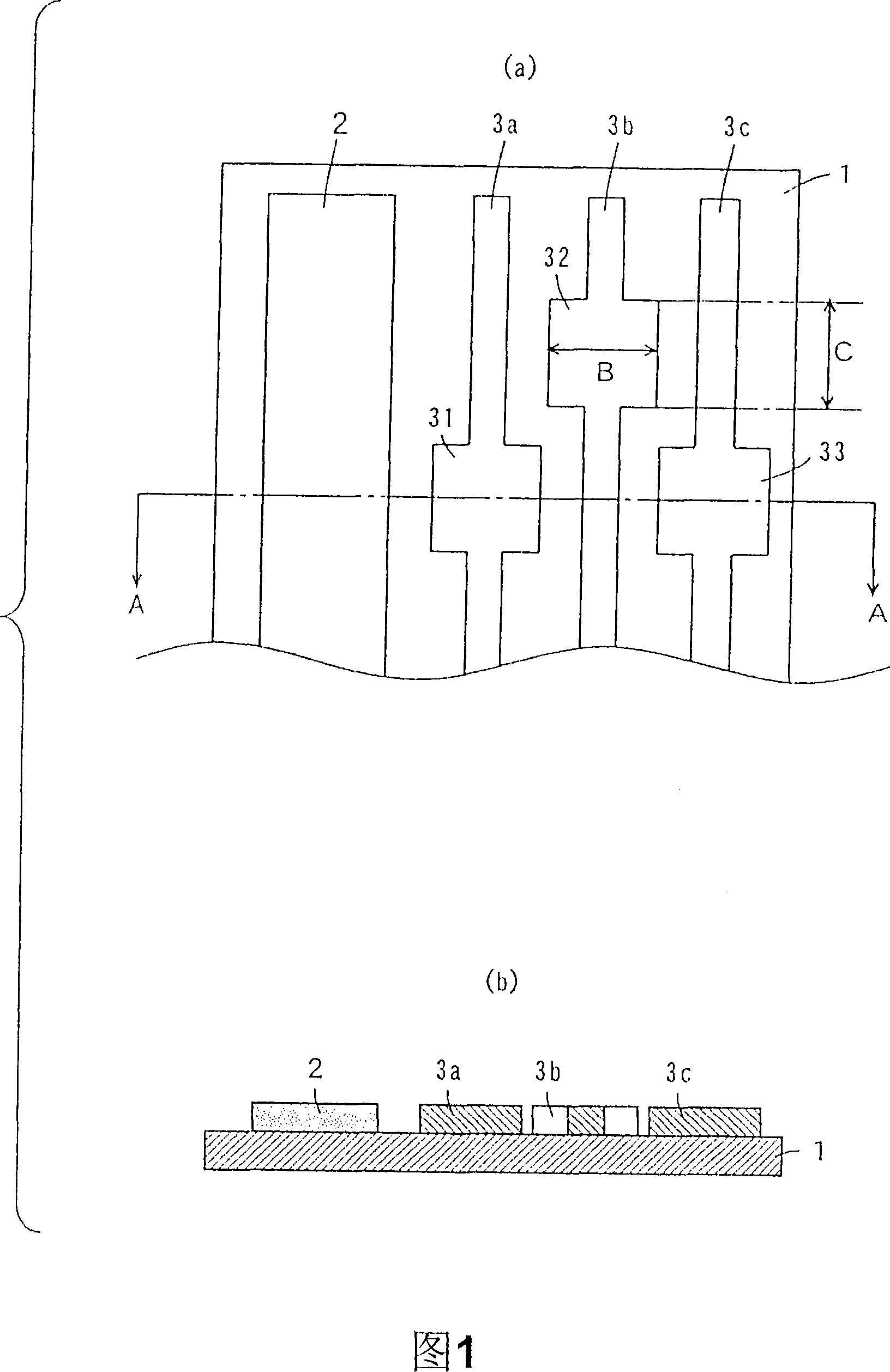
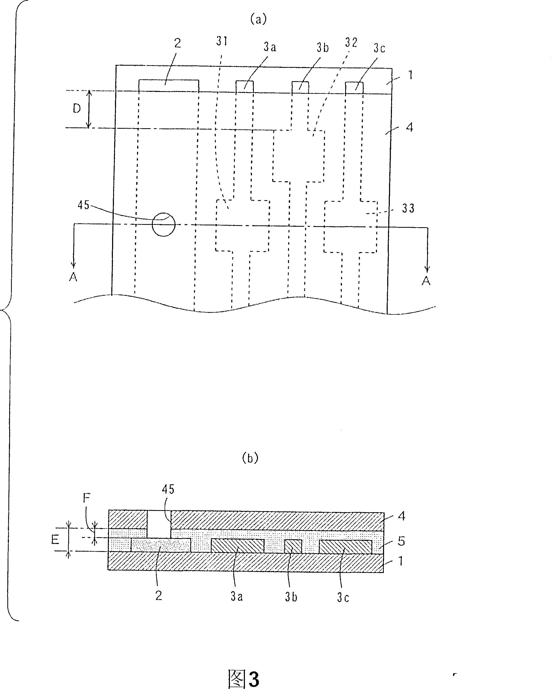
[0065] Fig. 7 is a top view showing the printed circuit board according to the first embodiment of the present invention. The printed circuit board 102 of FIG. 7 differs from the printed circuit board 101 of FIG. 6 in the following points. As shown in FIG. 7 , on printed circuit board 102 , wide portion 31 and wide portion 33 are arranged at positions closer to one end of first insulating cover layer 4 than wide portion 32 . In addition, the A-A line sectional view of the printed circuit board 102 is the same as that of FIG. 6( b ).

[0066] As the bottom insulating layer 1 of the printed circuit board 102, a polyimide resin having a thickness of 25 μm was used. The first to third signal lines 3 a to 3 c have a width of 0.2 mm and a thickness of 18 μm. The width B of the wide portions 31 to 33 is 3 mm, and the length C is 2 mm. The distance D between the wide portion 31 and the wide portion 33 and one end of the first insulating cover layer 4 was 5 mm.

[0067] In addition...

no. 2 example

[0070] The printed circuit board of the second embodiment differs from the printed circuit board 102 of FIG. 7 in the following points. In the printed circuit board of the second embodiment, the width B of the wide portions 31 to 33 is 1 mm, and the length C is 2 mm.

[0071] In the case of transmitting a high-frequency digital signal of 100 MHz using this printed circuit board, harmonics of 1280 MHz or higher can be removed, and high-frequency noise of 1280 MHz or higher does not occur.


PUM


Abstract

The present invention provides a printed circuit board includes a base insulating layer, first to third signal lines, a first cover insulating layer and a conductive layer. Wide parts are formed in the first to third signal lines. The first cover insulating layer is provided on the base insulating layer so as to cover the wide parts. The conductive layer is provided on the first cover insulating layer so as to cover a portion above the wide parts. A capacitive element is formed of the wide part, the cover insulating layer and the conductive layer. Generation of high-frequency noise can be prevented.

Description

technical field [0001] The present invention relates to a printed circuit board used in various electric and electronic devices. Background technique [0002] In recent years, as the digitalization of electric equipment, electronic equipment, etc. (hereinafter simply referred to as electronic equipment, etc.) progresses, higher functionality is also progressing. Along with this, the frequency of digital signals processed by electronic devices and the like has increased. [0003] In the case of processing digital signals on electronic devices and the like, high-frequency noise may be generated due to high harmonics. As a result, electronic devices and the like may malfunction. Therefore, in order to prevent the occurrence of high-frequency noise, a printed circuit board having a low-pass filter has been developed (for example, refer to JP-A-2004-254257). [0004] In the wiring board with a built-in low-pass filter described in JP-A-2004-254257, a low-pass filter is constit...

Claims


Application Information

Patent Timeline
Patent Type & Authority Applications(China)
IPC IPC(8): H05K1/02H03H1/00
CPCH05K1/162H05K1/0216H05K1/0218H05K2201/0715H05K2201/09727H05K3/4664H05K2201/09236
Inventor 本上满
Owner NITTO DENKO CORP
Why Eureka
Try Eureka