


Quick Research
Generate reliable direction feasibility study reports for your R&D in just a few steps.

Technical Q&A
Discover and master advanced knowledge NOW. Basics, ideas, possibilities, all at once.

Find Solutions
As an expert in R&D theories, this can generate solutions to your technical problems instantly.

Evaluate Feasibility
Analyze your overall solution with one click, know your potential R&D risks in advance.

Monitor Landscape
Get weekly tech updates, stay abreast of the latest tech innovations and key insights.
Flat display member and method for manufacturing same, and flat display and method for manufacturing same
A flat-panel display and a technology for a manufacturing method, which are applied in the manufacturing of flat-panel displays and flat-panel displays, components of flat-panel displays and their manufacture, and manufacturing of flat-panel displays, can solve problems such as complicated processes and increased costs, and achieve excellent production efficiency and electromagnetic wave shielding. Excellent effect
- Summary
- Abstract
- Description
- Claims
- Application Information
AI Technical Summary
Problems solved by technology
Method used
Image


Examples
Embodiment 1
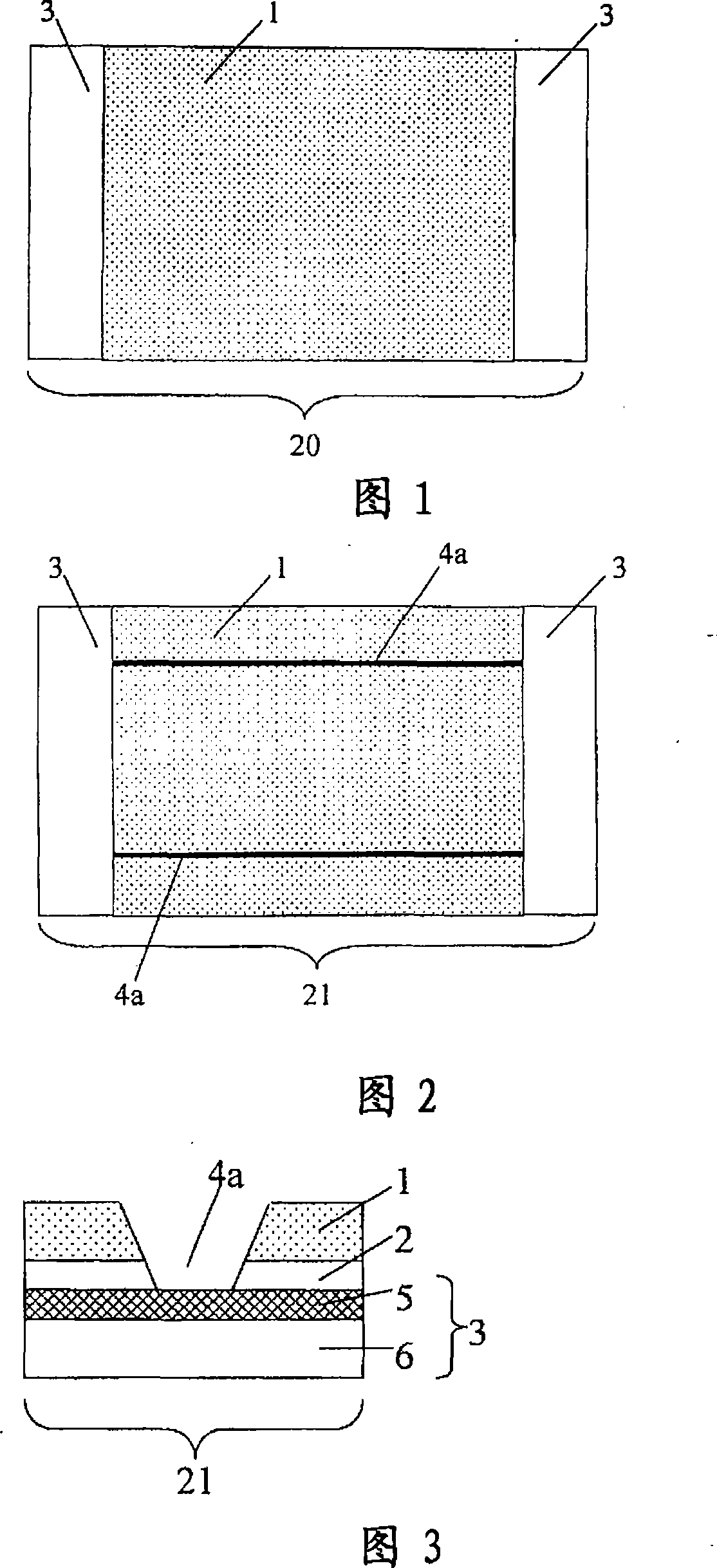
[0247] First, after peeling off the light-peeling PET film of the film-like adhesive material of 570 mm × 950 mm, the adhesive surface is bonded to the PET film of the anti-reflection film of 570 mm × 950 mm by using a sheet lamination device to align the end positions. On the film side, an antireflection film with an adhesive material is thus obtained. Then, peel off the heavy peeling treatment PET film of the film-like adhesive material of the anti-reflection film with the adhesive material, utilize the single-sheet lamination device to stick the copper mesh surface of the adhesive surface and the copper mesh film of 570mm * 980mm, by This gave a laminated body 1 . FIG. 1 shows a schematic plan view of a laminated body 1 of Example 1. As shown in FIG. The deviation of the end positions of the copper mesh film and the antireflection film with adhesive material at the peripheral portion of the laminate 1 of Example 1 was 0.2 mm on each of the two long sides, and 0.2 mm on eac...
Embodiment 2
[0252] A display member was obtained in the same manner as in Example 1 except that the laser irradiation conditions were an output of 30% and a laser head speed of 1300 cm / min. FIG. 2 shows a schematic plan view of the laminated body 2 of Example 2, and FIG. 5 shows a schematic cross-sectional view in the thickness direction of a portion where a void is formed. A void was formed from the outermost surface of the antireflection film (the outermost surface on the first surface side) to the PET film (transparent resin layer) of the copper mesh film, and the copper mesh was exposed in all directions.
[0253] 6 shows a schematic cross-sectional view in the thickness direction of the portion where the electrodes are formed in the flat-panel display component of the second embodiment. The electrodes are formed from the outermost surface of the antireflection film to the PET film of the copper mesh film. The average width of the electrode at the height position of the most surface ...
Embodiment 3
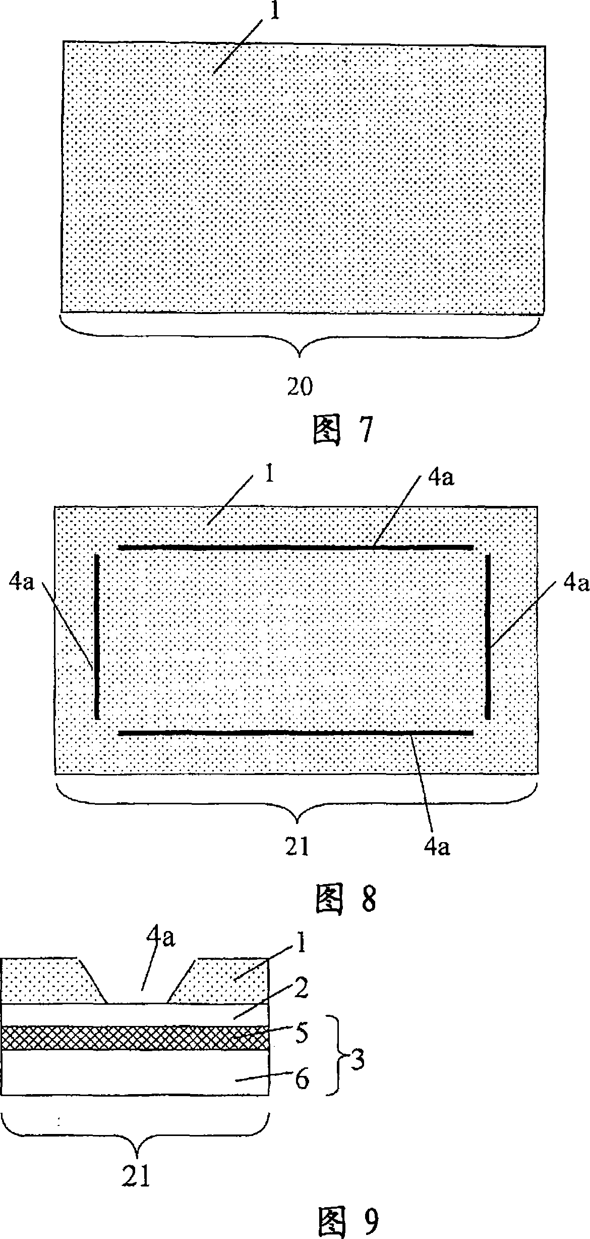
[0255] A laminate 1 was obtained in the same manner as in Example 1 except for using an antireflection film of 570 mm×980 mm and a film-shaped adhesive material of 570 mm×980 mm. FIG. 7 shows a schematic plan view of the laminated body 1 of Example 3. As shown in FIG. In Example 3, the maximum value of the positional deviation of the end portions of the copper mesh film and the antireflection film with adhesive in the peripheral portion of the laminate 1 was 0.3 mm.
[0256] Next, the laminated body 1 is fixed to a laser cutting machine. In the peripheral part of the laminated body 1, at the inner side of 10 mm from the end, the output is 20%, and the laser head speed is 1500 cm / min. In a linear shape with a length of 956 mm and a length of both short sides of 546 mm, a laser beam was irradiated from the surface of the laminate 1 on the antireflection film side to form voids to obtain a laminate 2 . FIG. 8 shows a schematic plan view of the laminated body 2 of Example 3, and ...
PUM
| Property | Measurement | Unit |
|---|---|---|
| width | aaaaa | aaaaa |
| distance | aaaaa | aaaaa |
| visible light transmittance | aaaaa | aaaaa |
Abstract
Description
Claims
Application Information
 - R&D Engineer
- R&D Manager
- IP Professional
- Industry Leading Data Capabilities
- Powerful AI technology
- Patent DNA Extraction
Browse by: Latest US Patents, China's latest patents, Technical Efficacy Thesaurus, Application Domain, Technology Topic, Popular Technical Reports.
© 2024 PatSnap. All rights reserved.Legal|Privacy policy|Modern Slavery Act Transparency Statement|Sitemap|About US| Contact US: help@patsnap.com