Programmable logic device fast logical block mapping method

A mapping method and programming logic technology, applied in the electronic field, can solve problems such as unacceptable running time, exponential increase in complexity, and incomparable performance

Inactive Publication Date: 2008-08-20
FUDAN UNIV
View PDF0 Cites 11 Cited by
  • Summary
  • Abstract
  • Description
  • Claims
  • Application Information

AI Technical Summary

Problems solved by technology

But the problem is that with the increase of the types of basic functional elements of the logic unit, the complexity of the algorithm increases exponentially, which is unacceptable in terms of running time
In addition, the performance of this algorithm cannot be compared with that of dedicated mapping algorithms.

Method used


Image

  • Programmable logic device fast logical block mapping method
  • Programmable logic device fast logical block mapping method
  • Programmable logic device fast logical block mapping method

Examples


Embodiment Construction

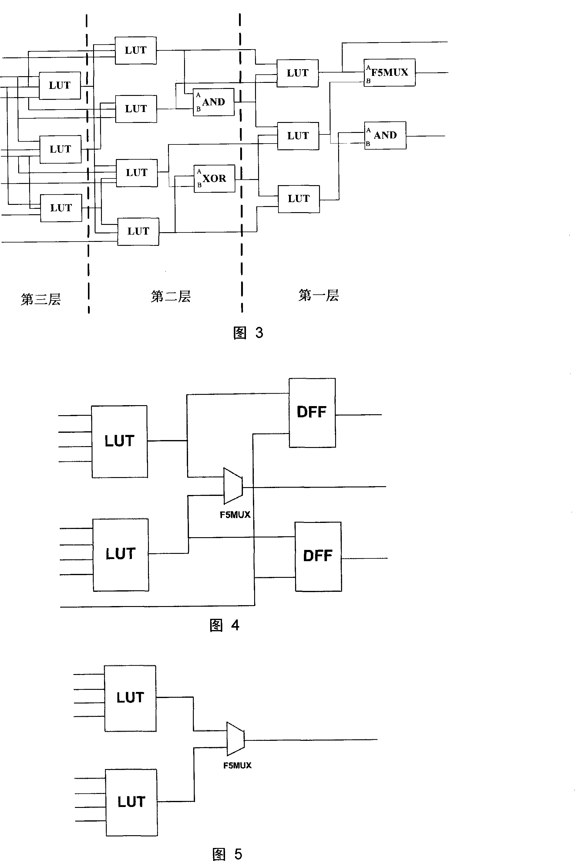
[0061] Figure 4 shows a simple use case of a user circuit. Here we take the chip structure of the SpartanII series as an example to introduce the entire matching mapping process.

[0062] Firstly, the sequential circuit part and the combined circuit part in the user circuit are separated, and the information of the sequential circuit part is stored. FIG. 5 is a schematic diagram showing the result after removing the sequential circuit part in the user circuit shown in FIG. 4 .

[0063] The next step is to map the remaining combinational and functional circuits in the user circuit.

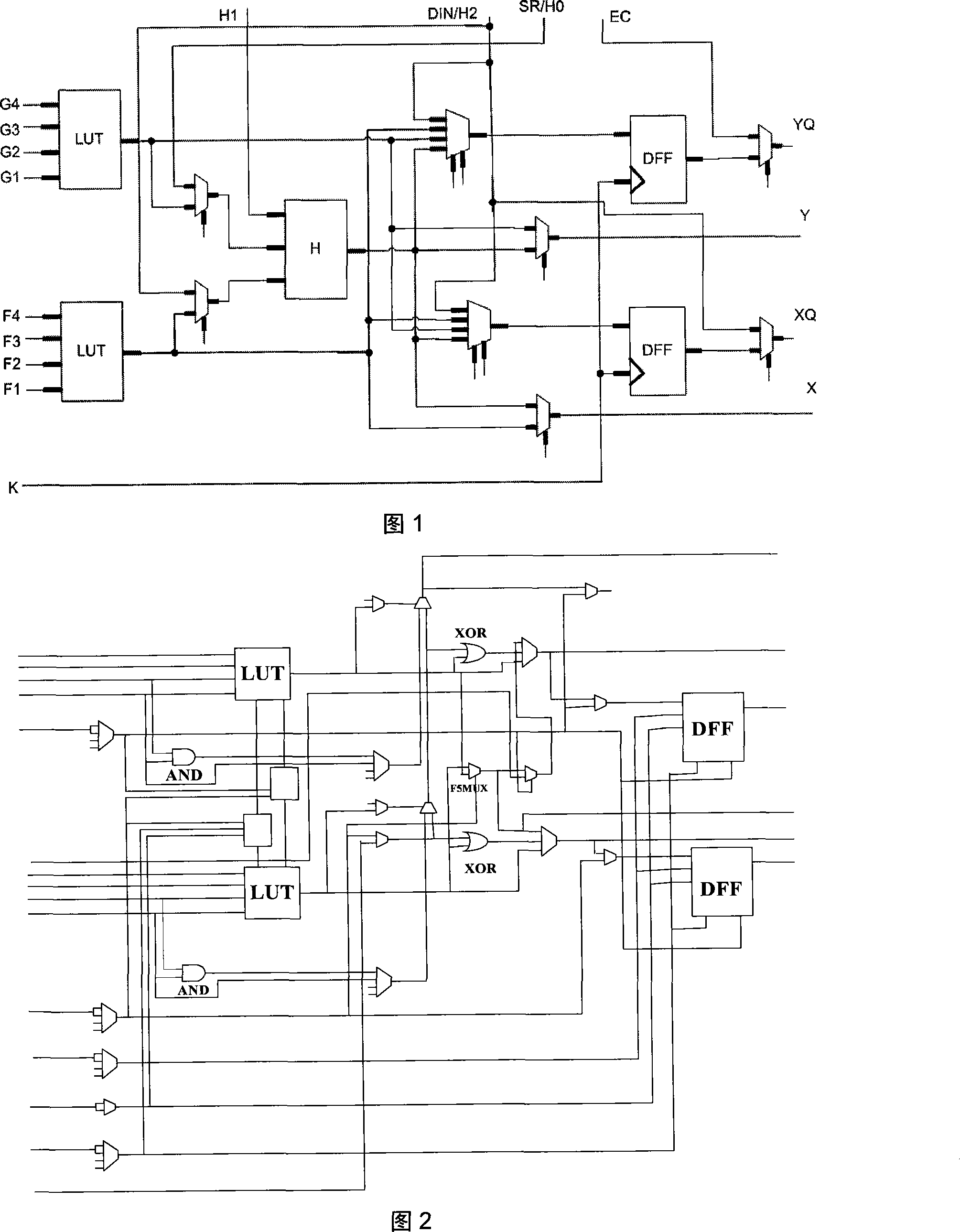
[0064] Figure 5 is also a functional circuit of the SpartanII series chips, which can be known by comparing Figure 2 and Figure 5. Figure 6 shows another functional circuit of the SpartanII series chips.

[0065] In the process of matching, 1) we can implement the user circuit with one SpartanII logic block unit as shown in FIG. 5 , and 2) it can also implement it with two logic block units as sh...


PUM


Abstract

The invention relates to a rapid logic mapping method for FPGA, belonging to the electronic technique field. A demixing and classification mapping to a programmable logic unit is raised to reduce the complexity of algorithm, a match degree coefficient is introduced to enhance the performance of the algorithm, and then a high performance rapid logic mapping method for FPGA is obtained. Experimental data show that the performance of the invention is enhanced by 12.59 percent compared to the conventional figure matching with the structure mapping algorithm, the complexity of algorithm is decreased largely from O(m) down to O(m), the invention can be widely applied in logic unit structure mapping for artery FPGA in modern times, the extendibility of FPGA logic unit mapping module in the operating efficiency and algorithm of the entire FPGA CAD flow is enhanced largely. The high performance rapid FPGA logic unit mapping method can also conduct the design of the FPGA programmable logic unit hardware structure, so that the structure advantages and disadvantages of the programmable logic unit can be estimated by the hardware design engineer before making chips, the design period is shortened largely, the success rate of a new device is increased, the design cost is saved.

Description

technical field [0001] The invention belongs to the field of electronic technology (Electronic Design Automation, EDA), and in particular relates to a software design and implementation method of a programmable logic device (FPGA) structure. technical background [0002] FPGA design includes its chip structure design and supporting software system design. Among them, the software system design must match the chip hardware structure. An efficient CAD system is a necessary condition for using FPGA. In traditional FPGA design, different hardware structures are often paired with different software algorithms: For example, the dedicated mapping algorithm lut2xc3k is used to process the programmable logic block PLB (Programming Logic Block) of XILINX XC3000 FPGA, and the dedicated mapping algorithm lut2xc4k is used to process XILINX XC4000 FPGA programmable logic unit, these two special algorithms are integrated in a system called RASP (Rapid System Prototyping) 【1】 . The direc...

Claims


Application Information

Patent Timeline
IPC IPC(8): G06F17/50
Inventor 来金梅蔡丹童家榕
Owner FUDAN UNIV
Why Eureka
Try Eureka