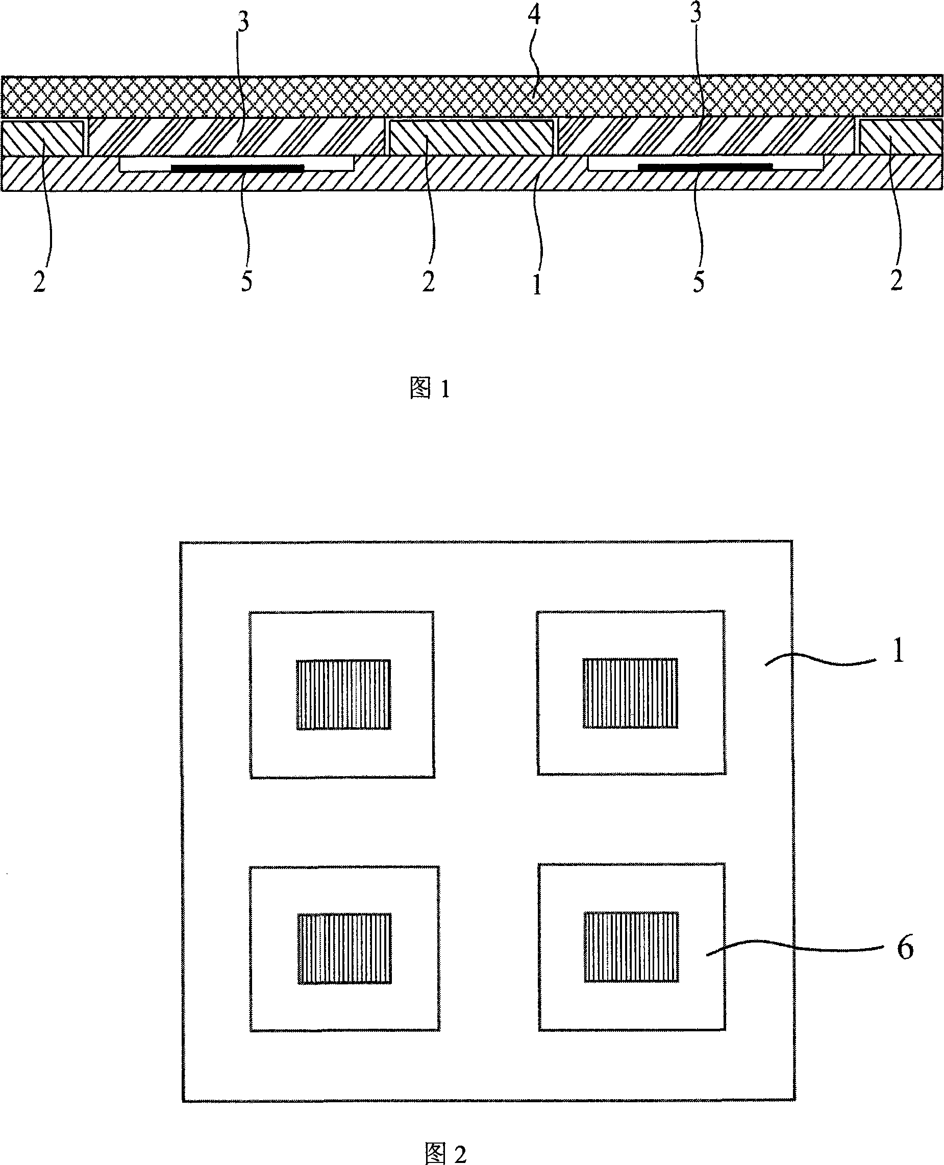
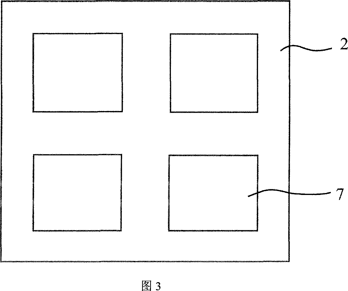
Novel packaging device of organic EL device and its packaging method
A technology of electroluminescent devices and packaging devices, which is applied in the direction of electric solid devices, electrical components, semiconductor devices, etc., to achieve the effect of simple structure and easy operation
- Summary
- Abstract
- Description
- Claims
- Application Information
AI Technical Summary
Problems solved by technology
Method used
Image
Examples
Embodiment approach 1-5
[0032] The preparation method is as follows:
[0033] ①Use detergent, ethanol solution and deionized water in sequence to ultrasonically clean the transparent conductive substrate ITO glass, and dry it with dry nitrogen after cleaning. The ITO film on the glass substrate is used as the anode layer of the device, the square resistance of the ITO film is 10-15Ω / □, and the film thickness is 1500 ;
[0034] ②Put the treated transparent substrate on the glue spinner to spin-coat the doped film (hole transport layer) PS:TPD, and roughly control the spin-coated film by controlling different solution concentration ratios, speed and time of the glue spinner. thickness of;
[0035] ③ Move the spin-coated substrate into a high vacuum chamber, and pretreat the ITO glass with low-energy oxygen plasma for 10 minutes in an oxygen environment with a pressure of 20Pa, and the sputtering power is ~20W;
[0036] ④Transfer the substrate to the organic vacuum evaporation chamber, and wait for ...
Embodiment approach 6-14
[0045] The preparation method is as follows:
[0046] ①Use detergent, ethanol solution and deionized water to ultrasonically clean the transparent conductive substrate ITO glass, and dry it with dry nitrogen after cleaning. The ITO film on the glass substrate is used as the anode layer of the device, the square resistance of the ITO film is 10-15Ω / □, and the film thickness is 1500 ;
[0047] ② Move the dried substrate into a high vacuum chamber, and pretreat the ITO glass with low-energy oxygen plasma for 10 minutes in an oxygen and argon atmosphere with a pressure of 20Pa, and the sputtering power is 20w;
[0048] ③Transfer the treated substrate to the organic vacuum evaporation chamber, and wait for the air pressure in the chamber to be 4×10 -4 Pa, the vapor deposition of the organic thin film is started. The hole injection layer evaporated sequentially according to the above device structure: CuPc is 200 , transport layer: α-NPD is 600 , light-emitting layer: Alq3 (...
Embodiment approach 15-20
[0054] The fabrication process of the device is similar to Embodiments 6-14.
[0055] Specific embodiments 21-30
PUM
 Abstract
Description
Claims
Application Information
 - R&D
- Intellectual Property
- Life Sciences
- Materials
- Tech Scout
- Unparalleled Data Quality
- Higher Quality Content
- 60% Fewer Hallucinations
Browse by: Latest US Patents, China's latest patents, Technical Efficacy Thesaurus, Application Domain, Technology Topic, Popular Technical Reports.
© 2025 PatSnap. All rights reserved.Legal|Privacy policy|Modern Slavery Act Transparency Statement|Sitemap|About US| Contact US: help@patsnap.com


