
Soldering pad structure in semiconductor apparatus and related method

A technology of semiconductors and pads, which is applied in the direction of semiconductor devices, semiconductor/solid-state device manufacturing, semiconductor/solid-state device components, etc., can solve the problems of reducing the overall performance of the chip, increasing the noise index, and reducing the noise immunity of the pads, etc.

Active Publication Date: 2010-04-14
FARADAY TECH CORP
View PDF1 Cites 0 Cited by
  • Summary
  • Abstract
  • Description
  • Claims
  • Application Information

AI Technical Summary

Problems solved by technology

In addition, the equivalent capacitance of the pad will also reduce the noise immunity (Noise immunity) of the pad to the substrate, resulting in an increase in the noise figure (Noise figure)
These negative effects will reduce the overall performance of the chip, especially for chips with high-speed application circuits, the reduction in chip performance will be more obvious

Method used


Image

  • Soldering pad structure in semiconductor apparatus and related method
  • Soldering pad structure in semiconductor apparatus and related method
  • Soldering pad structure in semiconductor apparatus and related method

Examples


Embodiment Construction

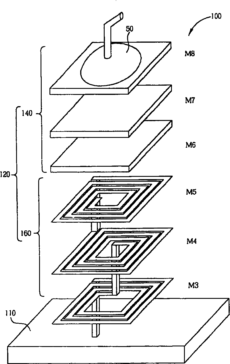
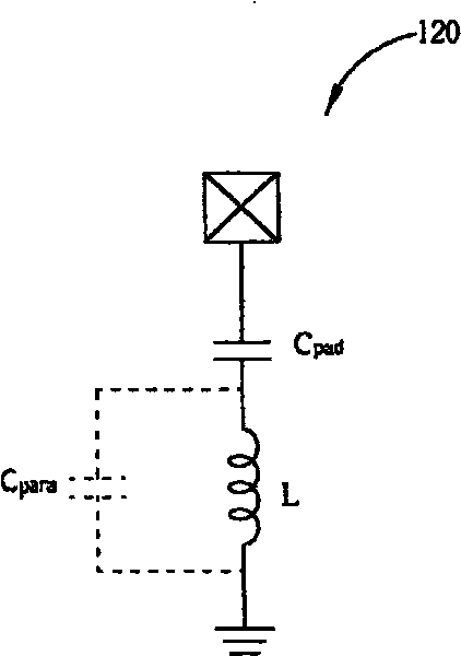
[0017] figure 1 It is a schematic diagram of the pad structure of the embodiment of the present invention. The bonding pad structure 120 of this embodiment is disposed in the semiconductor device 100 for electrically connecting the lead 50 to a core circuit (not shown) in the semiconductor device 100 . Wherein, the semiconductor device 100 includes a substrate 110 , and the bonding pad structure 120 includes a connection structure 140 and an inductor structure 160 .

[0018] The connection structure 140 is used to connect the lead 50 and the core circuit, so as to allow electrical signals to be transmitted between the lead 50 and the core circuit through the connection structure 140 . In this embodiment, the connection structure 140 includes three metal layers M6-M8 in total, wherein the metal layers M6 and M7 are connected to each other through one or more vias (Via), and the metal layers M7 and M8 are connected to each other through one or more vias. The holes are connecte...


PUM


Abstract

The invention discloses a welding pad structure which is arranged in a semiconductor device, and a method which is used for forming the welding pad structure. The semiconductor device comprises a base, and the welding pad structure comprises a connecting structure and an inductance structure. The connecting structure allows a lead wire to be connected on. The inductance structure is coupled with the connecting structure, and is used for reducing the equivalent capacitance value between the lead wire and the base.

Description

technical field [0001] The invention relates to a welding pad in a semiconductor device, in particular to a welding pad structure which can reduce the equivalent capacitance value between a lead and a substrate. Background technique [0002] Chips are one of the most common components in various electronic devices today. Generally speaking, a solid bonding pad must be provided on the chip, so that external leads (Bonding wire) can be electrically connected to the core circuit of the chip through the bonding pad. Through the bonding pads, the core circuit in the chip can transmit output signals to external circuits, or receive input signals transmitted from external circuits. In the known semiconductor process, in order to avoid the occurrence of the peel-off effect and ensure the reliability of the pad, multiple metal layers are generally used as the main structure of the pad. [0003] However, for the known pad structure, parasitic capacitance exists between every two adj...

Claims


Application Information

Patent Timeline
Patent Type & Authority Patents(China)
IPC IPC(8): H01L23/482H01L21/60
CPCH01L2224/04042H01L24/48H01L2924/01033H01L2924/01006H01L24/03H01L2924/01082H01L24/06H01L2924/01004H01L24/05H01L2224/48463H01L2924/014H01L2924/30107H01L2224/05554H01L2224/48
Inventor 柯明道萧渊文曾玉光
Owner FARADAY TECH CORP
Learn More