Structure of pad in IC and its formation process
A technology of integrated circuits and bonding wires, which is applied to the bonding pad structure of high-frequency, low-noise integrated circuits and its formation field, and can solve problems such as inability to isolate noise.
- Summary
- Abstract
- Description
- Claims
- Application Information
AI Technical Summary
Problems solved by technology
Method used
Image
Examples
Embodiment Construction
[0027] The invention discloses a structure of an integrated circuit bonding pad and a method for forming the same. Its specific embodiments are described with reference to the drawings, and similar reference numerals in the drawings represent similar components.
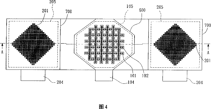
[0028] Please refer to FIG. 4 and FIG. 5 , which are structural schematic diagrams of a preferred embodiment of the integrated circuit bonding pad of the present invention. The structure of the integrated circuit bonding pad of the present invention is formed in an insulating layer 500 on a substrate 400. The structure of the integrated circuit bonding pad includes: a lower conductive layer 300, a composite layer structure 100 and a soldering layer. pad conductive layer 600 . The lower conductive layer 300 is arranged at a proper position in the insulating layer 500, and its two sides are respectively provided with a plurality of conductive layers 202 and a plurality of conductive connection layers 201 stacked on eac...
PUM
 Abstract
Description
Claims
Application Information
 - R&D Engineer
- R&D Manager
- IP Professional
- Industry Leading Data Capabilities
- Powerful AI technology
- Patent DNA Extraction
Browse by: Latest US Patents, China's latest patents, Technical Efficacy Thesaurus, Application Domain, Technology Topic, Popular Technical Reports.
© 2024 PatSnap. All rights reserved.Legal|Privacy policy|Modern Slavery Act Transparency Statement|Sitemap|About US| Contact US: help@patsnap.com


