


Quick Research
Generate reliable direction feasibility study reports for your R&D in just a few steps.

Technical Q&A
Discover and master advanced knowledge NOW. Basics, ideas, possibilities, all at once.

Find Solutions
As an expert in R&D theories, this can generate solutions to your technical problems instantly.

Evaluate Feasibility
Analyze your overall solution with one click, know your potential R&D risks in advance.

Monitor Landscape
Get weekly tech updates, stay abreast of the latest tech innovations and key insights.
Capacity controlled numerical frequency modulation circuit
A frequency modulation and circuit technology, applied in the field of electronics, can solve the problems of large chip area and increased system cost of flow control digital frequency modulation circuit
- Summary
- Abstract
- Description
- Claims
- Application Information
AI Technical Summary
Problems solved by technology
Method used
Image

Examples
specific Embodiment approach 1
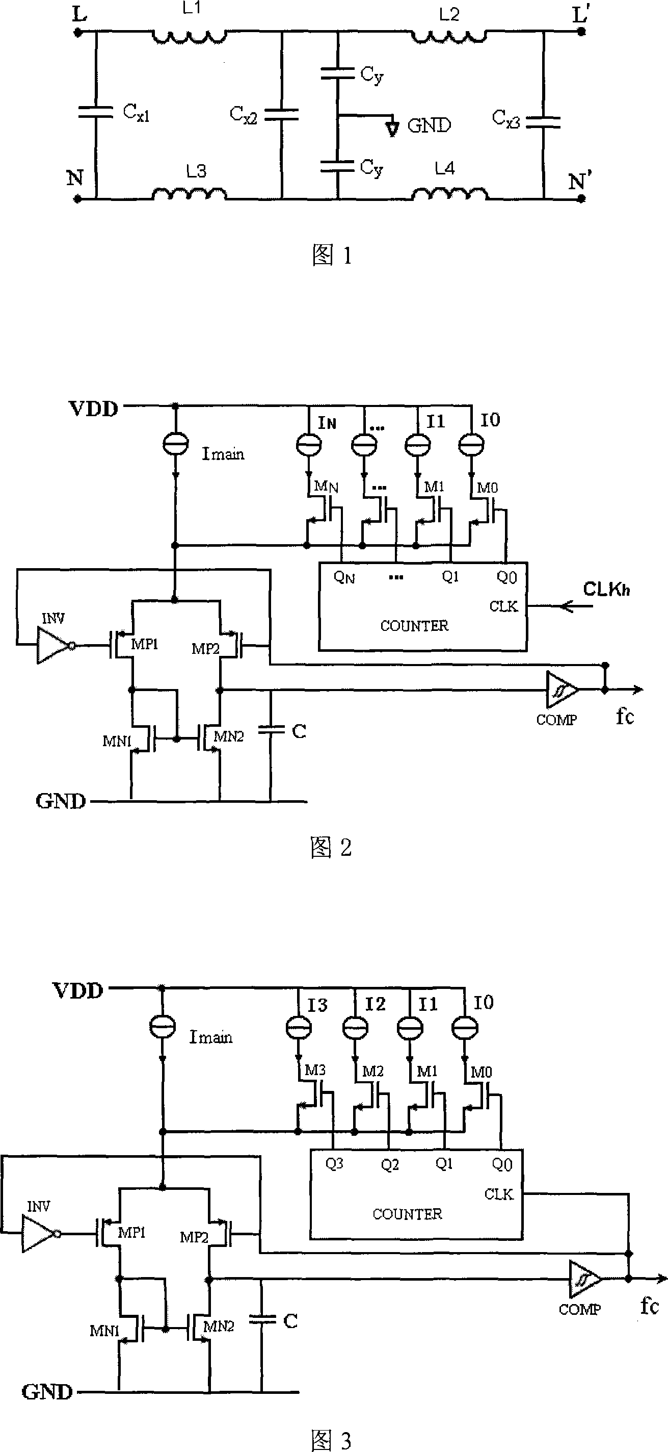
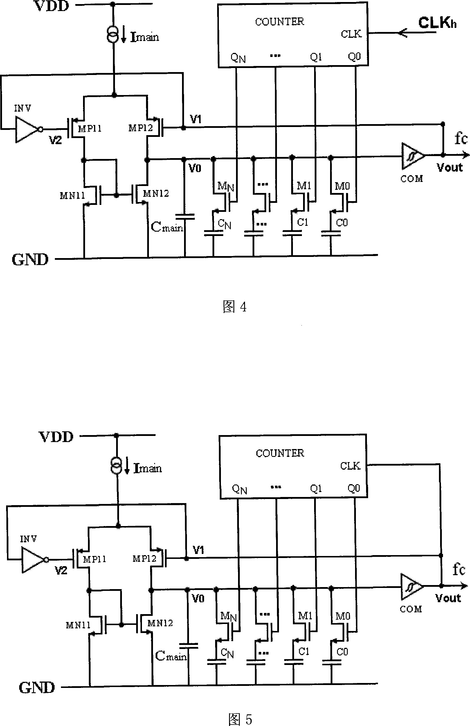
[0051] The capacitance-controlled digital frequency modulation circuit, as shown in Figure 6, includes a capacitor charging and discharging circuit, and the capacitor charging and discharging circuit is composed of an Imain current source, a PMOS differential input pair, an INV inverter, a current sink, and a COM hysteresis comparator constitute. The input terminal of the Imain current source is connected to the external power supply VDD, and its output terminal is connected to the sources of the PMOS transistor MP11 and the PMOS transistor MP12 of the PMOS differential input pair. The gate of the PMOS transistor MP11 is connected to the inverting output terminal of the INV inverter, and the gate of the PMOS transistor MP12 is connected to the non-inverting input terminal of the INV inverter and the comparison output terminal of the COM hysteresis comparator. Gates of the current sink NMOS transistor MN11 and NMOS transistor MN12 are interconnected, and their sources are groun...
specific Embodiment approach 2
[0052] Embodiment 1 In the scheme, the clock control signal CLKh input by the clock signal input terminal CLK of the N-bit COUNTER counter in the variable capacitance circuit can be provided by the oscillation frequency signal fc output by the entire capacity-controlled digital frequency modulation circuit, that is The comparison output terminal of the COM hysteresis comparator is connected to the clock signal input terminal CLK of the N-bit COUNTER counter, as shown in FIG. 7 .
specific Embodiment approach 3
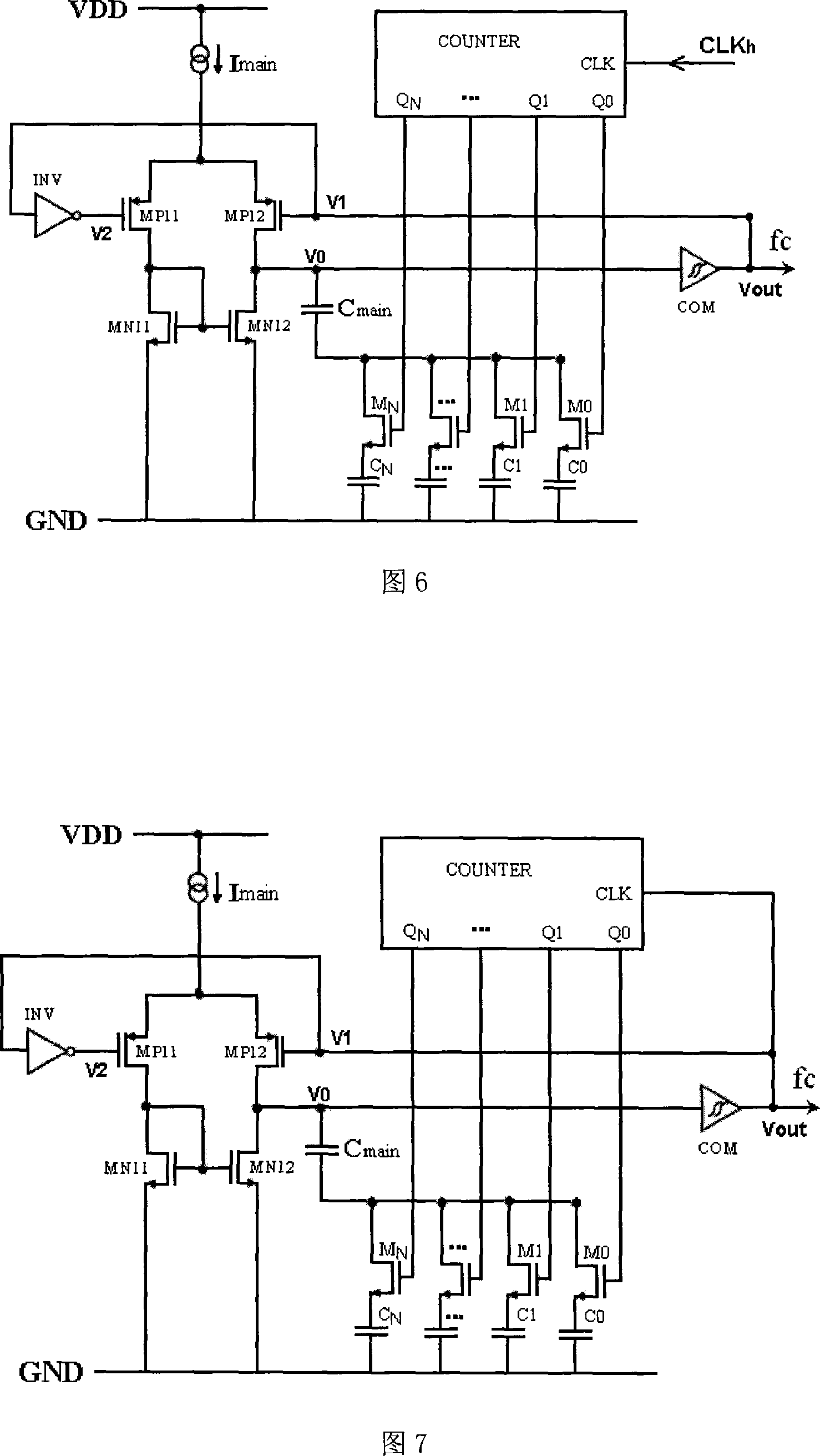
[0053] As shown in Figure 8, on the technical solution shown in Figure 5, the counting bit N of the N-bit COUNTER counter in the variable capacitance circuit is limited to 4, and the number of fine-tuning capacitors Ci (0≤i≤N) is 4 , that is, there are four trimming capacitors C0, C1, C2 and C3, and the number of NMOS switch transistors Mi (0≤i≤N) is 4, that is, there are four NMOS switch transistors M0, M1, M2 and M3.
[0054] Similar, also can be on the technical scheme shown in Fig. 4, Fig. 6 and Fig. 7, limit the value of the count position N of the N-bit COUNTER counter in the variable capacitance circuit to be 4, fine-tune capacitance Ci (0≤i≤N ) is 4, that is, there are four trimming capacitors C0, C1, C2 and C3, and the number of NMOS switch tubes Mi (0≤i≤N) is 4, that is, there are four NMOS switches M0, M1, M2 and M3 Tube, thus designing different implementations.
PUM
 Abstract
Description
Claims
Application Information
 - R&D Engineer
- R&D Manager
- IP Professional
- Industry Leading Data Capabilities
- Powerful AI technology
- Patent DNA Extraction
Browse by: Latest US Patents, China's latest patents, Technical Efficacy Thesaurus, Application Domain, Technology Topic, Popular Technical Reports.
© 2024 PatSnap. All rights reserved.Legal|Privacy policy|Modern Slavery Act Transparency Statement|Sitemap|About US| Contact US: help@patsnap.com