Method for manufacturing three-dimensional nerve microelectrode
A manufacturing method and micro-electrode technology, applied in the direction of micro-structure technology, micro-structure devices, manufacturing micro-structure devices, etc., can solve the problems of large influence of insulating layer process, easy to generate pinholes, unfavorable long-term implantation, etc., and achieve production cost The effect of reducing and eliminating pinholes and good consistency of electrical characteristics
- Summary
- Abstract
- Description
- Claims
- Application Information
AI Technical Summary
Problems solved by technology
Method used
Image

Examples
Embodiment 1
[0025] In this embodiment, the cylindrical hole 8 made of SU-8 glue has a height of 100 micrometers and is used for sticking on the surface of the dura mater of the optic nerve or cerebral cortex to stimulate the optic nerve or cerebral cortex to restore nerve function.
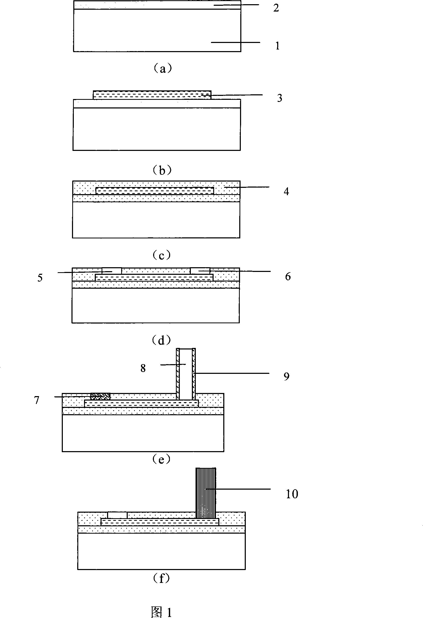
[0026] As shown in Figure 1, this embodiment includes the following steps:
[0027] Step 1, clean the silicon wafer 1, use the silicon wafer 1 as the substrate, and use PECVD (plasma chemical vapor deposition) method to grow the bottom SiO on the polished surface of the silicon wafer 1 2 2. Bottom SiO2 2 2 is used to electrically isolate the metal alloy layer from the silicon substrate, as shown in Figure 1(a).
[0028] The silicon wafer 1 is N-type single crystal silicon.
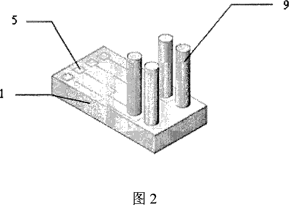
[0029] Step 2, on the bottom SiO 2 Metal titanium and gold are sequentially sputtered on 2 to form a metal alloy layer, and metal interconnection lines 3, pads 5 and contact dots 6 are etched out. Dot 6 is used to electroplate and gro...
Embodiment 2
[0036] In this embodiment, the cylindrical hole 8 made of SU-8 glue has a height of 500 micrometers and is used to penetrate the dura mater and stick on the surface of the pia mater to stimulate the optic nerve or cerebral cortex to restore nerve function.
[0037] As shown in Figure 1, this embodiment includes the following steps:
[0038] Step 1, clean the silicon wafer 1, use the silicon wafer 1 as the substrate, and use PECVD (plasma chemical vapor deposition) method to grow the bottom SiO on the polished surface of the silicon wafer 1 2 2. Bottom SiO2 2 2 is used to electrically isolate the metal alloy layer from the silicon substrate, as shown in Figure 1(a).
[0039] The silicon wafer 1 is P-type single crystal silicon.
[0040] Step 2, on the bottom SiO 2 Metal titanium and gold are sequentially sputtered on 2 to form a metal alloy layer, and metal interconnection lines 3, pads 5 and contact dots 6 are etched out. Dot 6 is used to electroplate and grow cylindrical ...
Embodiment 3
[0047] The height of the cylindrical hole 8 that adopts SU-8 glue to form among the present embodiment is 1 millimeter, is used for penetrating dura mater and pia mater, punctures in optic nerve or cerebral cortex, is used for stimulating optic nerve or cerebral cortex, carries out neural Functional fixes.
[0048] As shown in Figure 1, this embodiment includes the following steps:
[0049] Step 1, clean the silicon wafer 1, use the silicon wafer 1 as the substrate, and use PECVD (plasma chemical vapor deposition) method to grow the bottom SiO on the polished surface of the silicon wafer 1 2 2. Bottom SiO2 2 2 is used to electrically isolate the metal alloy layer from the silicon substrate, as shown in Figure 1(a).
[0050] The silicon wafer 1 is N-type single crystal silicon.
[0051] Step 2, on the bottom SiO 2 Metal titanium and gold are sequentially sputtered on 2 to form a metal alloy layer, and metal interconnection lines 3, pads 5 and contact dots 6 are etched out. ...
PUM
| Property | Measurement | Unit |
|---|---|---|
| height | aaaaa | aaaaa |
| height | aaaaa | aaaaa |
Abstract
Description
Claims
Application Information
 - R&D
- Intellectual Property
- Life Sciences
- Materials
- Tech Scout
- Unparalleled Data Quality
- Higher Quality Content
- 60% Fewer Hallucinations
Browse by: Latest US Patents, China's latest patents, Technical Efficacy Thesaurus, Application Domain, Technology Topic, Popular Technical Reports.
© 2025 PatSnap. All rights reserved.Legal|Privacy policy|Modern Slavery Act Transparency Statement|Sitemap|About US| Contact US: help@patsnap.com