


Quick Research
Generate reliable direction feasibility study reports for your R&D in just a few steps.

Technical Q&A
Discover and master advanced knowledge NOW. Basics, ideas, possibilities, all at once.

Find Solutions
As an expert in R&D theories, this can generate solutions to your technical problems instantly.

Evaluate Feasibility
Analyze your overall solution with one click, know your potential R&D risks in advance.

Monitor Landscape
Get weekly tech updates, stay abreast of the latest tech innovations and key insights.
Semiconductor device
A semiconductor and conductivity-type technology, applied in the direction of semiconductor devices, transistors, electric solid-state devices, etc., can solve problems such as difficult device integration, unstable threshold voltage of NMOSFET and PMOSFET, terminals formed on one surface, etc., and achieve the goal of reducing on-resistance Effect
- Summary
- Abstract
- Description
- Claims
- Application Information
AI Technical Summary
Problems solved by technology
Method used
Image

Examples
no. 1 approach
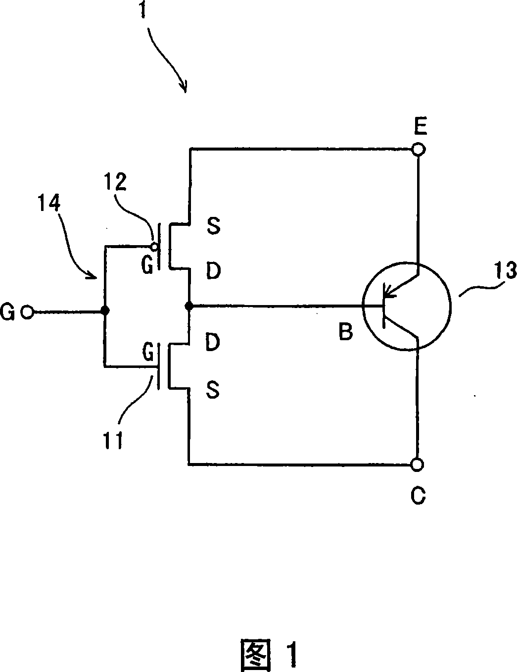
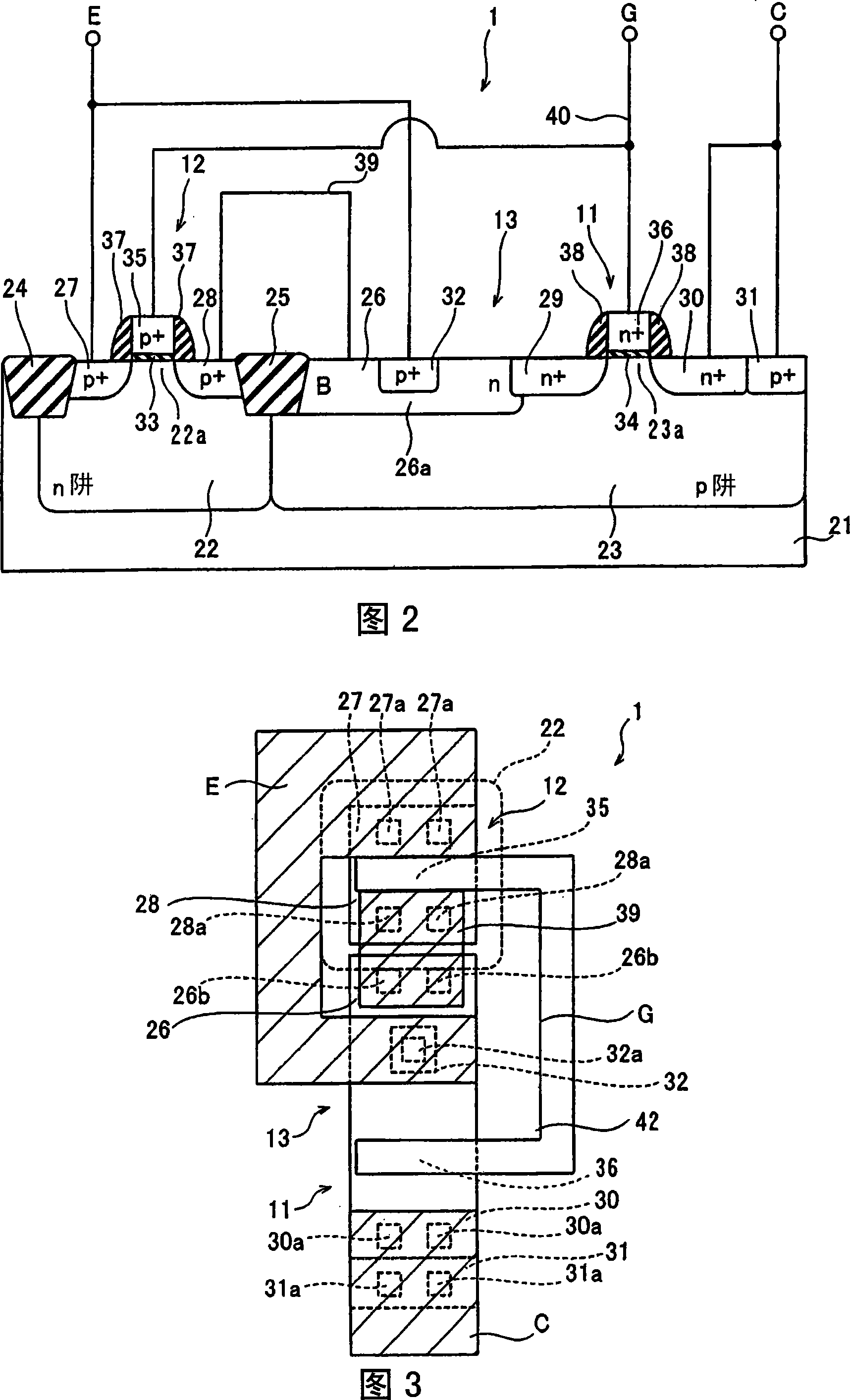
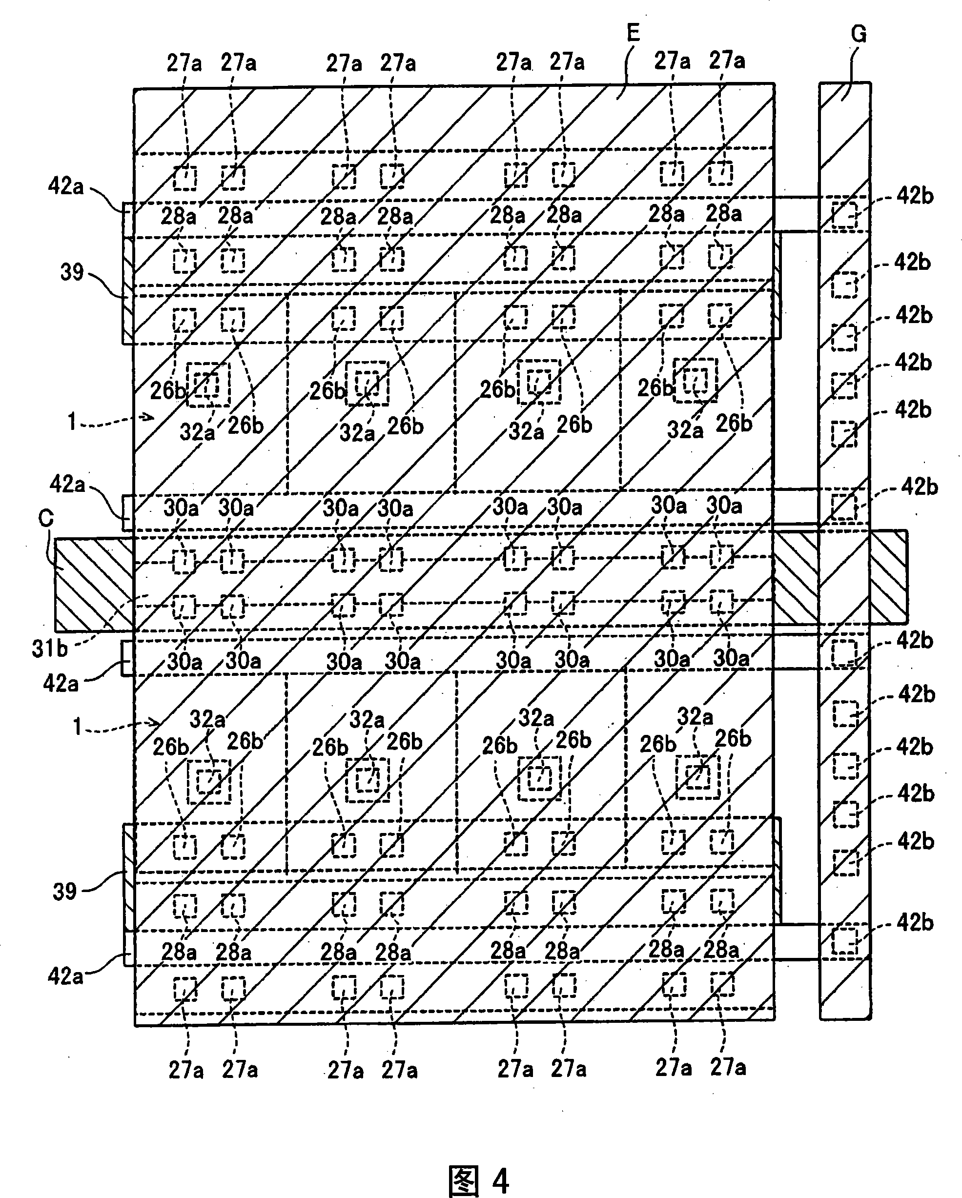
[0084] FIG. 1 is a circuit diagram of a semiconductor device according to a first embodiment of the present invention. FIG. 2 is a cross-sectional view of the semiconductor device of the first embodiment shown in FIG. 1 . 3 is an electrode arrangement diagram of the semiconductor device of the first embodiment shown in FIG. 1 . 4 is an electrode arrangement diagram when the semiconductor devices of the first embodiment shown in FIG. 1 are arranged in an array. First, the configuration of a semiconductor device according to a first embodiment of the present invention will be described with reference to FIGS. 1 to 4 .
[0085] The semiconductor device 1 of the first embodiment includes an NMOSFET 11 , a PMOSFET 12 , and a pnp bipolar transistor 13 as shown in FIG. 1 . In addition, NMOSFET11 is an example of the "first conductivity type first field effect transistor" of this invention, and PMOSFET12 is an example of "second conductivity type second field effect transistor" of t...
no. 2 approach
[0100] 7 is a cross-sectional view of a semiconductor device according to a second embodiment of the present invention. Referring to FIG. 7 , a description will be given of a semiconductor device in which the surface of the semiconductor substrate and the upper portion of the gate electrode are silicided in this second embodiment, which is different from the first embodiment described above.
[0101] In the semiconductor device of the second embodiment, as shown in FIG. 7, p + source region 27, p + Type gate electrode 35, p + Drain region 28, n-type base layer 26, p + Emitter layer 32, n + Drain region 29, n + Type gate electrode 36, n + source region 30 and p + The surface of the collector layer 31 is silicided to form metal silicide films 41a to 41g. In this way, the n-type base layer 26, p + source region 27, p + Drain region 28, n + Drain region 29, n + Source region 30, p + collector layer 31 and p + The surface of each impurity region of the emitter layer 32...
no. 3 approach
[0113] 16 is a cross-sectional view of a semiconductor device according to a third embodiment of the present invention. Referring to FIG. 16 , in this third embodiment, unlike the above-described second embodiment, n well 22 and p well 23 are formed in deep n well 51 (deep n well: DNW). As a result, the diffusion current to the p-type silicon substrate 21 in the collector current of the pnp-type bipolar transistor 13 can be suppressed, so that the current can be collected more effectively in the p-type silicon substrate 21. + collector layer 31 . As a result, the on-resistance of the pnp-type bipolar transistor 1 can be reduced. In addition, the n well 51 is an example of the "second well region" in the present invention.
[0114] In addition, other effects of the third embodiment are the same as those of the second embodiment described above.
PUM
 Abstract
Description
Claims
Application Information
 - R&D Engineer
- R&D Manager
- IP Professional
- Industry Leading Data Capabilities
- Powerful AI technology
- Patent DNA Extraction
Browse by: Latest US Patents, China's latest patents, Technical Efficacy Thesaurus, Application Domain, Technology Topic, Popular Technical Reports.
© 2024 PatSnap. All rights reserved.Legal|Privacy policy|Modern Slavery Act Transparency Statement|Sitemap|About US| Contact US: help@patsnap.com