
Packaging structure for luminescent device

A light-emitting device and packaging structure technology, which is applied in the direction of electrical components, electric solid-state devices, circuits, etc., can solve the problems of ineffective expansion of the viewing angle range of the optical path, reduced utilization rate of the light-emitting device, waste, etc., to achieve the best visual brightness, Effect of increasing electric power and reducing fluctuation

Inactive Publication Date: 2008-01-02
深圳市健隆新光电技术有限公司
View PDF6 Cites 0 Cited by
  • Summary
  • Abstract
  • Description
  • Claims
  • Application Information

AI Technical Summary

Problems solved by technology

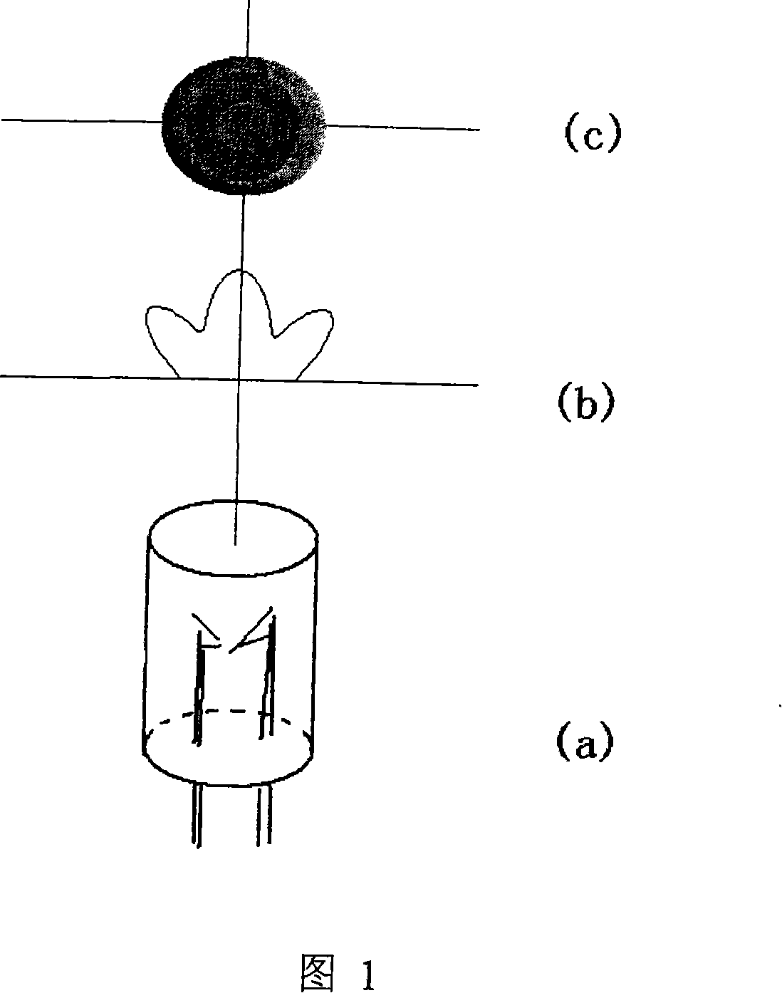
[0012] To sum up, since the viewing angle range of a person and the display screen are basically in a horizontal observation position, people hardly observe a luminous object from top to bottom or from bottom to top (vertical direction), and the disclosure in the above-mentioned prior art The cross-section of the shell of the light-emitting diode is circular, which determines that the light-emitting chip located in the center emits a light source to the surrounding (horizontal and vertical directions) and the light-emitting angle is uniform and the same. The light emitted above is wasted in vain, and the light emission angle in the horizontal direction is limited by the viewing angle of the circular section, which limits the viewing angle range of people, the visual effect is not good and the utilization rate of the light emitting device is greatly reduced; In order to change the distribution of light in the horizontal direction and vertical direction, the side wall of the housing is set in the form of a plurality of lens curved surfaces to improve the utilization rate of the light emitting device, but the manufacturing process of the housing with this structure is very difficult , the design requirements are high, and it also has a series of parameter requirements. In addition, the shell of this structure has no obvious effect on expanding the viewing angle range of the optical path. In view of the above-mentioned defects in the prior art, the technicians of the present invention have continuously studied , to develop a packaging structure of light-emitting devices that can change the optical path and save costs, and has a simple manufacturing process

Method used


Image

  • Packaging structure for luminescent device
  • Packaging structure for luminescent device
  • Packaging structure for luminescent device

Examples


Embodiment 1

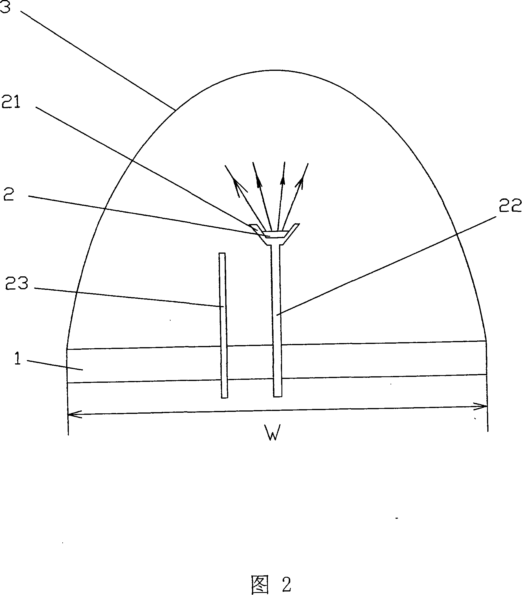
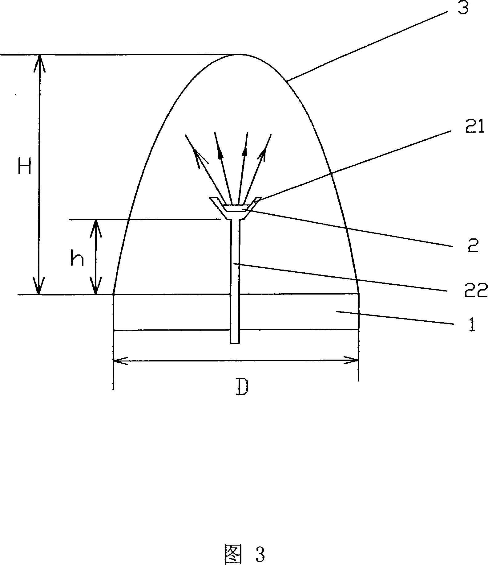
[0037] In the packaging structure of the light-emitting device, the total height H of the diode housing 3 is preferably 7MM, the length W of the diode housing 3 in the horizontal direction is preferably 3.9MM, and the width D of the diode housing 3 in the vertical direction is The most is 3.1MM.

[0038] As shown in Figure 4, when the light emission angle a of the light emitting diode chip 2 in the horizontal direction is 100 degrees and the light emission angle a in the vertical direction is 40 degrees, the light emitting diode chip 2 and the tube base The best distance h between 1 is 4.5MM.


PUM


Abstract

A package structure of lighting device comprises an integrated tubular base with high thermal conductivity, at least one light emitting diode chip, and a diode casing, which are packed integrally. The lighting diode chip is fixed in a support disc which bottom is arranged with a pin lead wire, the lighting device is arranged with an internal lead wire, the section of the diode casing is ellipse. The distance between the lighting diode chip and the tubular base can be adjusted to adjust the light emitting angle of the lighting diode chip. The inventing can reduce the fluctuation of lighting strength from center to edge, which lens unit can be produced via integral injection made method, with simple production. The invention has best vision brightness, without affecting vision and increasing power.

Description

technical field [0001] The present invention relates to a packaging structure of a light emitting device, in particular to a packaging structure of a light emitting device suitable for display, with substantially uniform luminous intensity within the range of the cylinder projection of the light emitting device. Background technique [0002] The light-emitting body of the light-emitting device is mainly made of compound semiconductors such as gallium phosphide. The light-emitting principle uses electric energy to apply current to the compound, and through the combination of electrons and holes, the energy is released in the form of light. [0003] Since the light of the light-emitting device is cold light, the life of the light-emitting device is more than 100,000 hours, and the response speed is fast, so it can be used in many fields such as large-scale displays, traffic lights, and mobile phones. [0004] However, the light of the light-emitting device is directional, and ...

Claims


Application Information

Patent Timeline
Patent Type & Authority Applications(China)
IPC IPC(8): H01L33/00H01L25/00H01L25/075H01L25/13H01L23/04H01L23/055H01L23/31H01L33/54H01L33/58
Inventor 熊毅伟
Owner 深圳市健隆新光电技术有限公司
Learn More