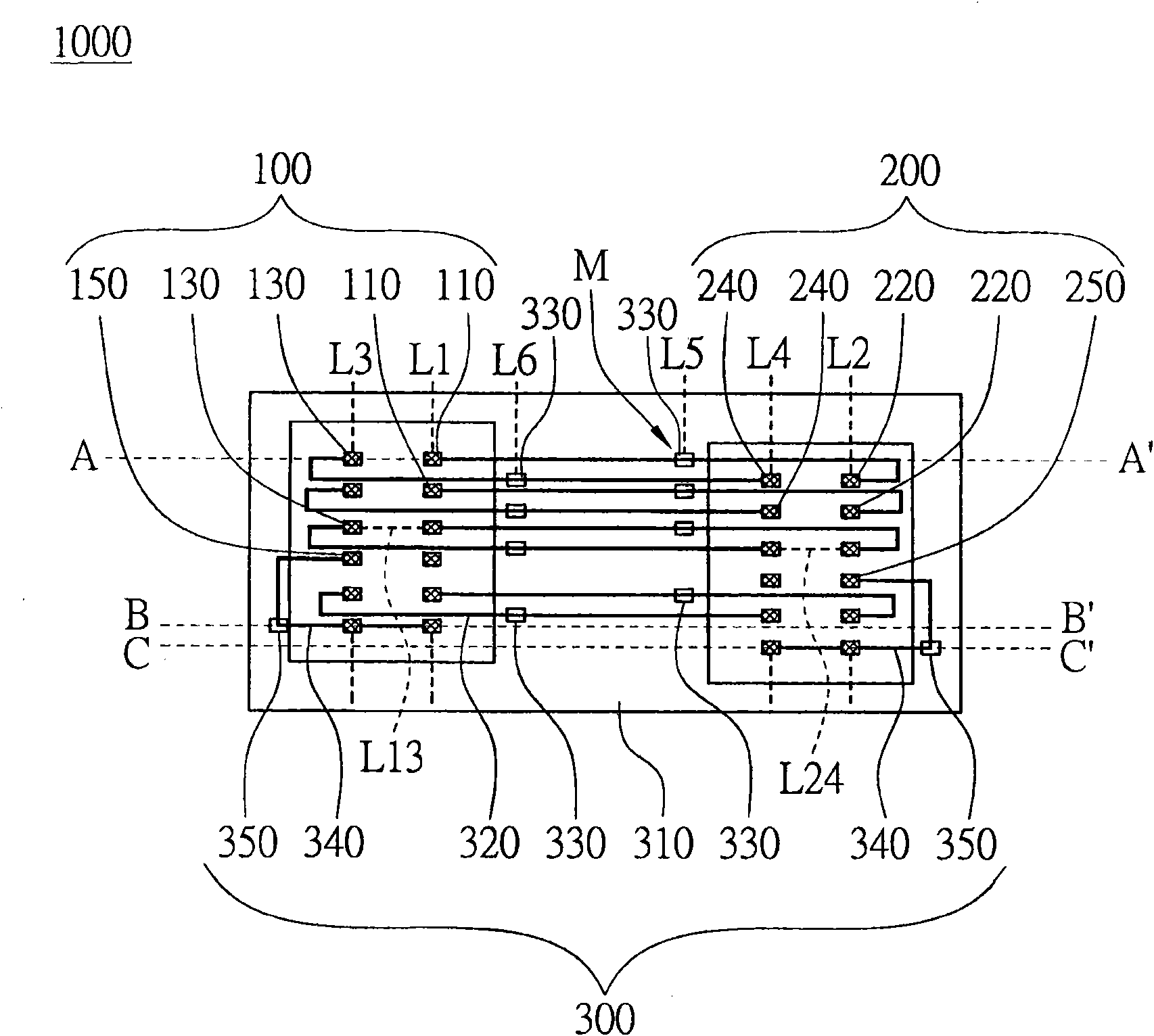
Package Structure
A packaging structure, semiconductor technology, applied in electrical components, electrical solid devices, circuits, etc., can solve problems such as difficulty in wire design
- Summary
- Abstract
- Description
- Claims
- Application Information
AI Technical Summary
Problems solved by technology
Method used
Image
Examples
no. 1 example
[0058] Please refer to figure 1 , which shows a schematic diagram of the packaging structure 1000 according to the first embodiment of the present invention. The packaging structure 1000 of this embodiment includes a first semiconductor element 100, a second semiconductor element 200, a semiconductor connecting element 300 (Interposer) (the material of which includes thermoplastic resin (thermoplastic) or epoxy resin (epoxy)) and a substrate 400. The first semiconductor element 100 and the second semiconductor element 200 are, for example, memory chips, processing chips, or photosensitive chips. In this embodiment, both the first semiconductor device 100 and the second semiconductor device 200 are memory chips, and the circuit structures of the first semiconductor device 100 and the second semiconductor device 200 are the same. The material of the substrate 400 is an insulating material, such as glass fiber (FR4) or ceramic material. The semiconductor connecting element 300...
no. 2 example
[0082] Please refer to Figure 5 , which shows a top view of the package structure 2000 according to the second embodiment of the present invention. The package structure 2000 of this embodiment differs from the package structure 1000 of the first embodiment in the configuration of the power supply wire 340a, and the rest of the similarities will not be described again.
[0083] Such as Figure 5 As shown, the semiconductor connection element 300a of this embodiment includes several power supply wires 340a, and one end of each power supply wire 340a is connected to a power supply conductive bump 150 or a power supply conductive bump 250, and is adjacent to the power supply conductive bump 150 or the power supply conductive bump 250. The power conductive bump 250 is provided. The other end of each power wire 340 a is connected to each respective power conductive post 350 . In this way, the length of each power wire 340a can be shortened to the minimum, so that the impedance ...
no. 3 example
[0085] Please refer to Figure 6 , which shows a top view of the package structure 3000 according to the third embodiment of the present invention. The packaging structure 3000 of this embodiment differs from the packaging structure 2000 of the second embodiment in the number of the first semiconductor elements 100 and the number of the second semiconductor elements 200 , and the rest of the similarities will not be repeated.
[0086] Such as Figure 6 As shown, the package structure 3000 includes several first semiconductor devices 100 and several second semiconductor devices 200 . The numbers of the first semiconductor elements 100 and the second semiconductor elements 200 are the same. And the first semiconductor elements 100 correspond to the second semiconductor elements 200 one by one.
[0087] When the first semiconductor device 100 and the second semiconductor device 200 are similar, the semiconductor connection device 300b can reproduce the patterns of multiple set...
PUM
 Abstract
Description
Claims
Application Information
 - R&D
- Intellectual Property
- Life Sciences
- Materials
- Tech Scout
- Unparalleled Data Quality
- Higher Quality Content
- 60% Fewer Hallucinations
Browse by: Latest US Patents, China's latest patents, Technical Efficacy Thesaurus, Application Domain, Technology Topic, Popular Technical Reports.
© 2025 PatSnap. All rights reserved.Legal|Privacy policy|Modern Slavery Act Transparency Statement|Sitemap|About US| Contact US: help@patsnap.com


