
Picture processing apparatus, imaging apparatus and method of the same

A technology of image processing equipment and imaging equipment, applied in image communication, conversion of storage devices with different read and write speeds, television, etc., can solve the problems of manufacturing cost, increase in circuit size and power consumption, etc. The effect of cost containment

Inactive Publication Date: 2007-12-26
SONY CORP
View PDF1 Cites 13 Cited by
  • Summary
  • Abstract
  • Description
  • Claims
  • Application Information

AI Technical Summary

Problems solved by technology

As a result, there are problems of increased manufacturing cost, circuit size, and power consumption

Method used


Image

  • Picture processing apparatus, imaging apparatus and method of the same
  • Picture processing apparatus, imaging apparatus and method of the same
  • Picture processing apparatus, imaging apparatus and method of the same

Examples


no. 1 example

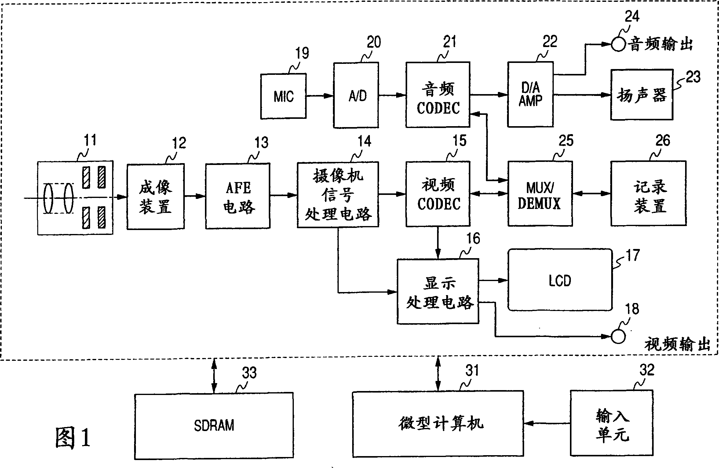
[0032] FIG. 1 is a block diagram of the configuration of an imaging apparatus according to a first embodiment of the present invention.

[0033] The imaging device shown in FIG. 1 is a so-called digital video camera that images a moving image and records the imaged image as digital data in a recording medium.

[0034] This imaging device includes an optical block 11, an imaging device 12, an analog front end (AFE) circuit 13, a camera signal processing circuit 14, a video CODEC (coder / decoder) 15, a display processing circuit 16, an LCD (liquid crystal display) 17, a video Output terminal 18, microphone 19, A / D converter 20, audio CODEC 21, D / A (digital / analog) conversion amplifier 22, speaker 23, audio output terminal 24, MUX / DEMUX (multiplexer / demultiplexer ) 25, recording device 26, microcomputer 31, input unit 32, and SDRAM (Synchronous Dynamic Random Access Memory) 33.

[0035] The optical block 11 includes a lens for collecting light from a subject to the imaging device 1...

no. 2 example

[0088] In the first embodiment described above, the playback compatibility of the recorded image data is ensured by recording the image data as HD images at 30 fps in the high-speed imaging mode. However, in the second embodiment, image data recorded in the high-speed imaging mode is recorded as an image at 120 fps at the same refresh rate as that at the time of imaging.

[0089] FIG. 7 is an explanatory diagram of a signal flow at the time of recording an image in the second embodiment.

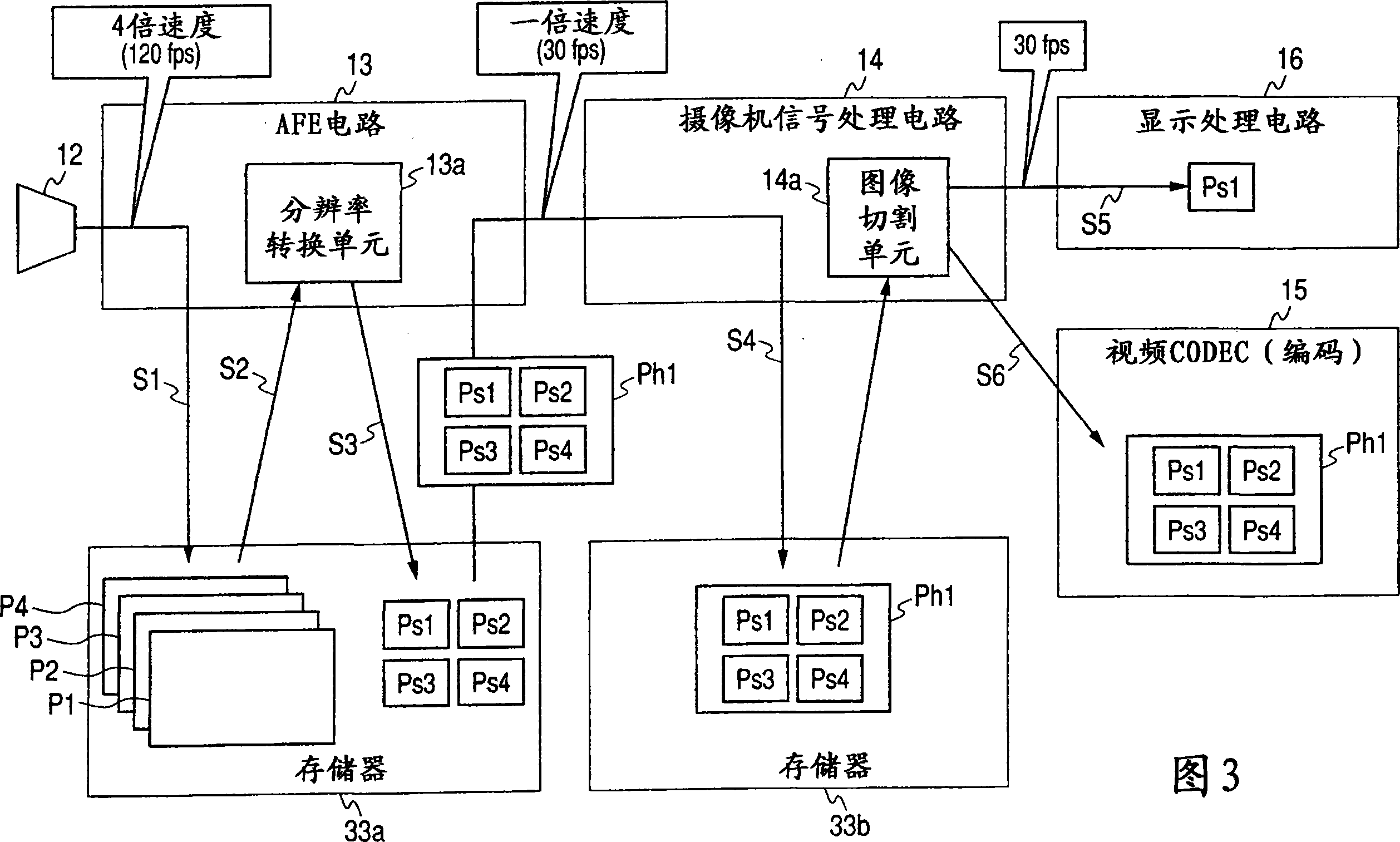
[0090] In FIG. 7, images are imaged at 120 fps from the imaging device 12, these images are converted into SD images, and 4 SD images are merged into one HD image until the image quality correction (step Steps S31 to S34) are the same as the first embodiment in FIG. 3 (steps S1-S4).

[0091] Next, the image cutting unit 14a reads out the HD image in which four SD images are combined from the storage area 33b, and then cuts out each area of ​​the SD image from the HD image. After that, one ...


PUM


Abstract

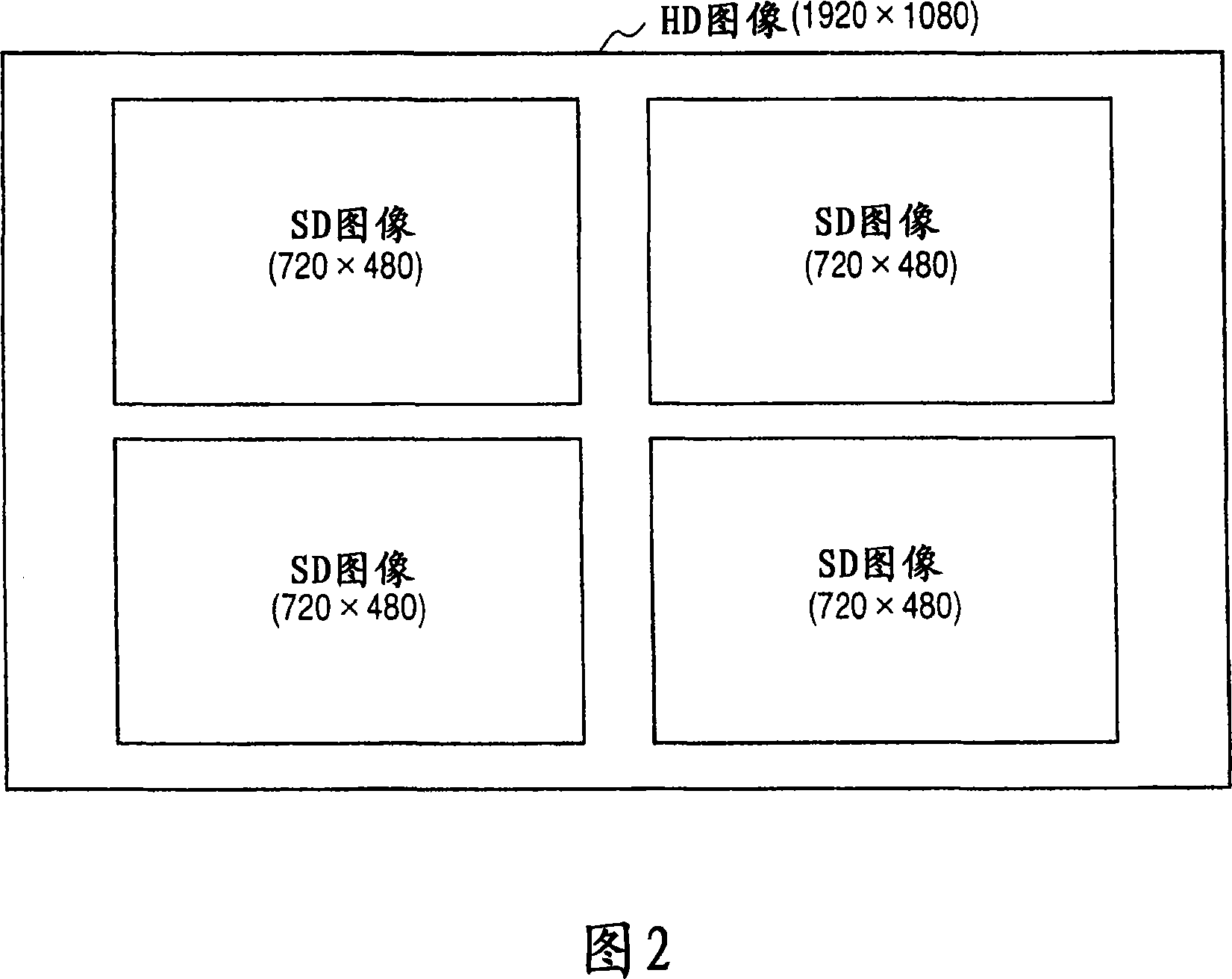
An imaging apparatus which images pictures using a solid-state imaging device includes a picture conversion unit converting pictures imaged at a high-speed screen rate by the solid-state imaging device into a picture in which n-pieces (''n'' is an integer of 2 or more) of continuous imaged pictures are arranged in one screen and outputting the converted picture at a low-speed screen rate which is 1 / n of the high-speed screen rate, a signal processing unit performing predetermined picture-quality compensation processing to the picture from the picture conversion unit, a display picture cutting unit cutting one of n-pieces of imaged pictures from pictures processed by the signal processing unit and outputting the picture at the low-speed screen rate, and a display processing unit generating picture signals for displaying the picture outputted from the display picture cutting unit at a display device.

Description

[0001] Cross References to Related Applications [0002] The present invention contains subject matter of Japanese Patent Application JP 2006-172974 filed in the Japan Patent Office on Jun. 22, 2006, the entire content of which is hereby incorporated by reference. technical field [0003] The present invention relates to an image processing device for processing image signals, an imaging device for imaging images by using a solid-state imaging device, and a processing method in these devices, and more particularly, the present invention relates to an An image processing device for an image signal, an imaging device and a method thereof. Background technique [0004] In recent years, advances in the capabilities of imaging devices and signal processing technologies have enabled consumer digital video cameras capable of shooting and recording at higher resolutions than the existing NTSC (National Television Standards Committee) standard. HDTV (High Definition Television) stan...

Claims


Application Information

Patent Timeline
Patent Type & Authority Applications(China)
IPC IPC(8): H04N5/225H04N7/015H04N5/92H04N23/40
CPCH04N5/85H04N5/783H04N5/772H04N5/45H04N5/781H04N7/0105H04N9/8063H04N21/42203H04N21/4325H04N5/775H04N21/440281H04N9/8042H04N21/440263H04N21/4223H04N21/4334H04N5/44591H04N9/7921H04N21/4316H04N7/0806H04N5/23293H04N21/42692H04N7/0125H04N21/47H04N23/63H04N23/815H04N25/42H04N5/915H04N5/9202
Inventor 木村正成
Owner SONY CORP
Learn More