Planar display device with H-shaped sided-grid controlled structure and its production
A flat panel display and manufacturing process technology, applied in the control electrodes, the manufacture of discharge tubes/lamps, and image/graphic display tubes, etc., can solve the problems of high gate voltage and large gate current, etc.
Inactive Publication Date: 2010-11-24
ZHONGYUAN ENGINEERING COLLEGE
View PDF0 Cites 0 Cited by
- Summary
- Abstract
- Description
- Claims
- Application Information
AI Technical Summary
Problems solved by technology
In most of the current display devices, the control mode in which the gate structure is located above the carbon nanotube cathode structure is adopted. The advantage is that the control effect of the gate structure is relatively significant, but the gate voltage remains high, so The formed gate current is somewhat large, which is its disadvantage and needs further improvement
Method used
View moreImage
Smart ImageViewing Examples

Examples
Embodiment Construction
Login to View More PUM
 Abstract
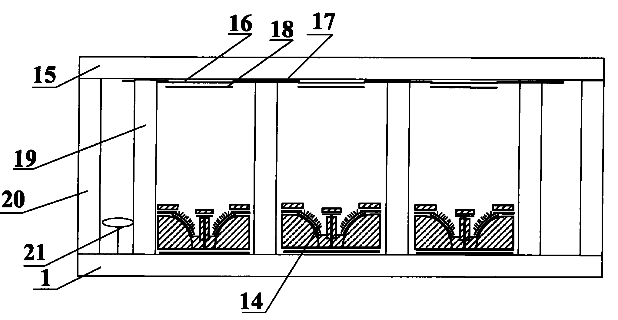
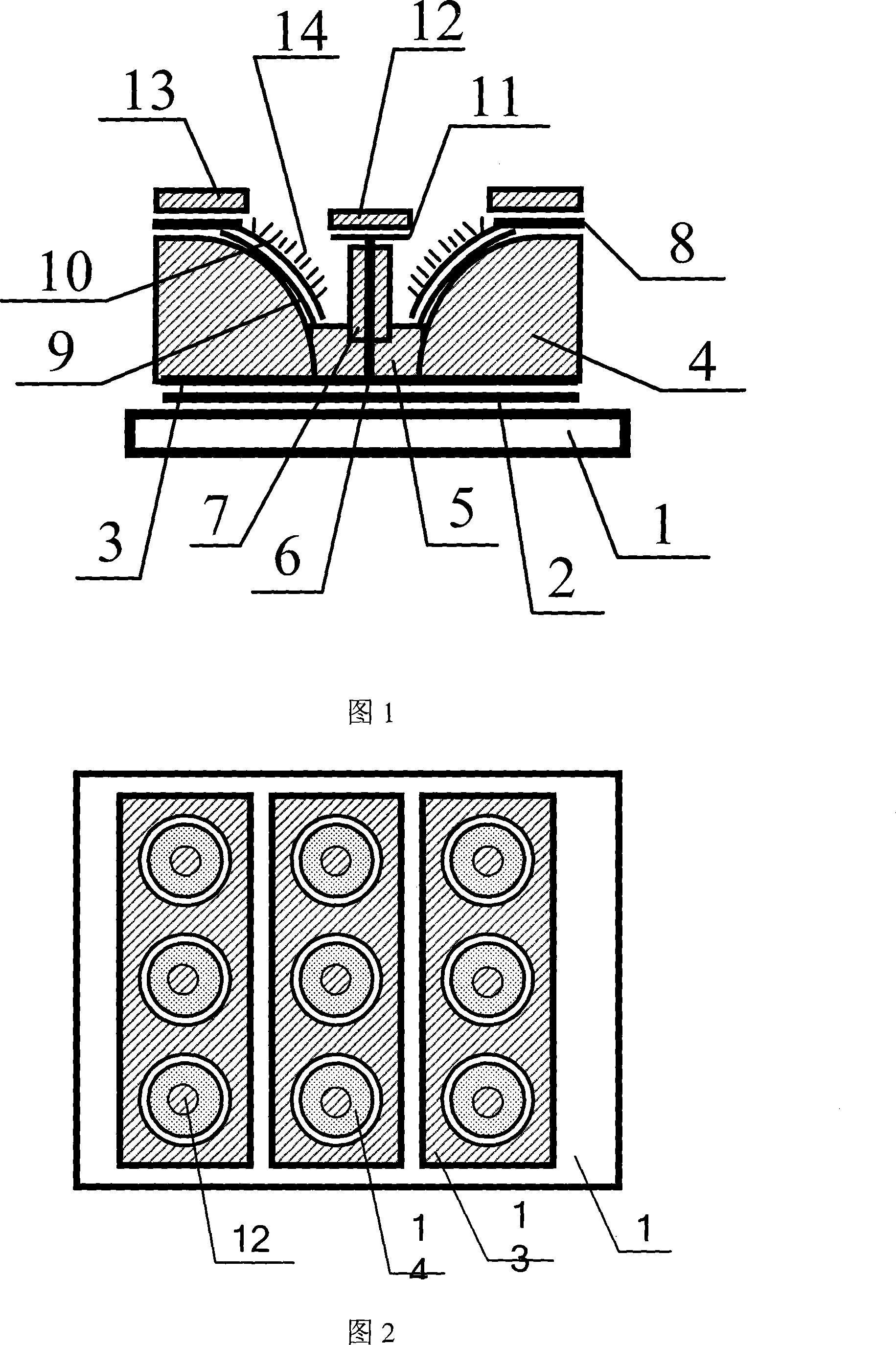
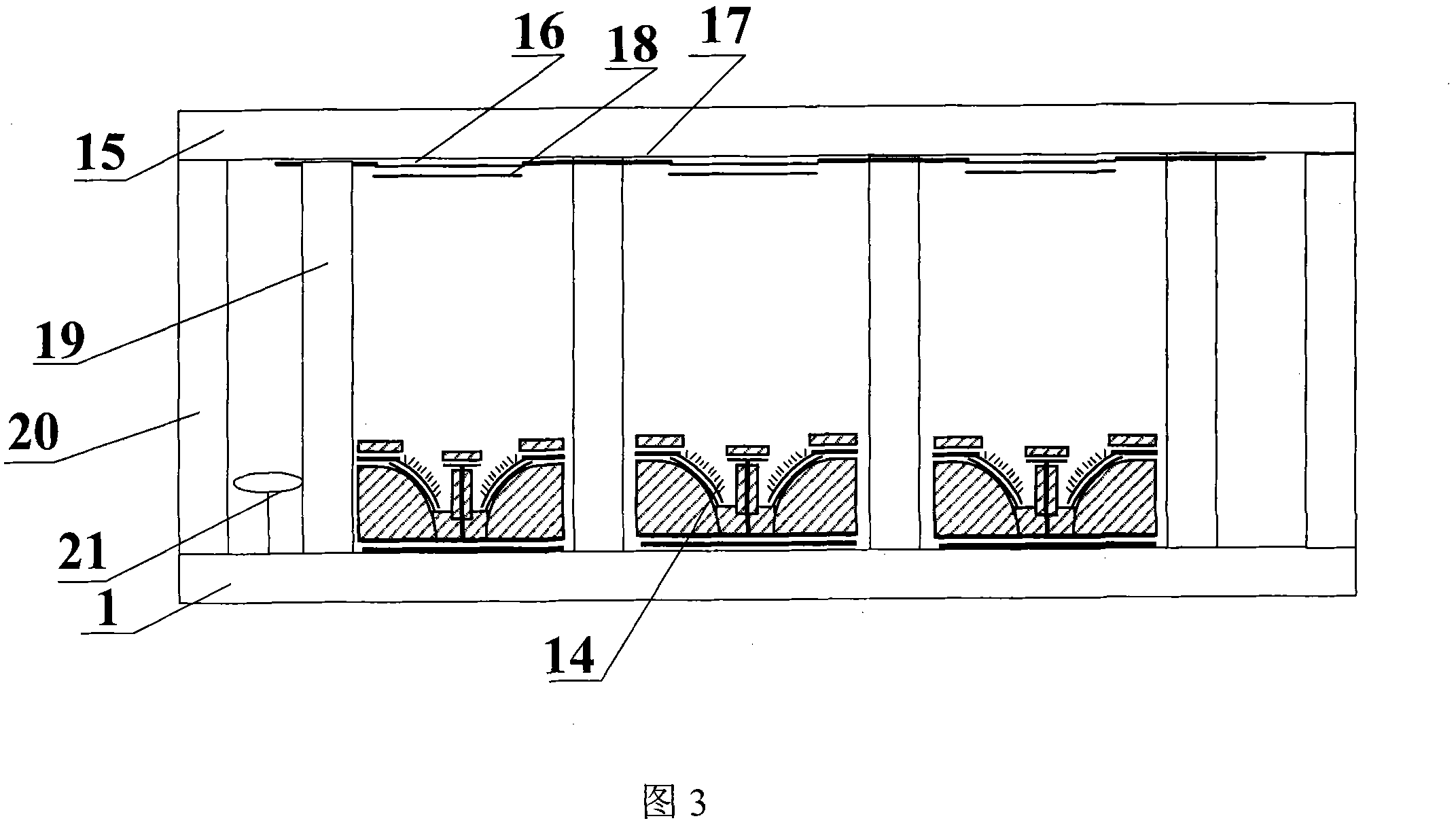
This is a flat displayer of I shape side grid cathode structure and its production process. It includes a sealed vacuum chamber formed by a anodic glass panel, a cathode glass panel and surrounded glass frame; on the anodic glass panel is a conducting layer coated with fluorescent; a supporting wall between the anodic and cathode panel and a getter; on the cathode glass panel are a grid down-leadlayer, carbon nanotube and I shape side grid structure, which is capable of increasing the electron ejecting area and efficiency of the nanotube and increasing the control function of the grid.
Description
Flat panel display with I-shaped side gate control structure and its manufacturing process technical field The invention belongs to the fields of flat panel display technology, microelectronic science and technology, vacuum science and technology, and nano science and technology, and relates to device fabrication of flat panel field emission displays, in particular to carbon nanotube cathodes. The device manufacturing aspect of the flat panel field emission display particularly relates to a flat panel display with an I-shaped side gate control structure and its manufacturing process. Background technique Carbon nanotube cathode field emission display is a new type of flat panel display device, which makes full use of the cold field emission characteristics of carbon nanotubes, and uses the strength of an external electric field to force the tip of carbon nanotubes to emit electrons instead of using thermal energy to make field emission The energy distribution of the electr...
Claims
Login to View More Application Information
Patent Timeline
 Patent Type & Authority Patents(China)
IPC IPC(8): H01J31/12H01J31/15H01J29/02H01J29/04H01J1/304H01J1/46H01J9/02H01J9/00
Inventor 李玉魁
Owner ZHONGYUAN ENGINEERING COLLEGE
Features
- R&D
- Intellectual Property
- Life Sciences
- Materials
- Tech Scout
- Unparalleled Data Quality
- Higher Quality Content
- 60% Fewer Hallucinations
Learn More Browse by: Latest US Patents, China's latest patents, Technical Efficacy Thesaurus, Application Domain, Technology Topic, Popular Technical Reports.
© 2025 PatSnap. All rights reserved.Legal|Privacy policy|Modern Slavery Act Transparency Statement|Sitemap|About US| Contact US: help@patsnap.com