Optical multilayer filter, method for manufacturing the same, and electronic apparatus
A technology of optical multilayer film and manufacturing method, which is applied in the direction of optics, optical components, and optical filters for photography, and can solve the problems of unfavorable cost and changing the optical characteristics of optical multilayer film filters, etc.
- Summary
- Abstract
- Description
- Claims
- Application Information
AI Technical Summary
Problems solved by technology
Method used
Image
Examples
Embodiment 1~7、 comparative example 1~7
[0037] The present embodiment is an example suitable for an optical multilayer film filter (UV-IR cut filter) which passes the visible wave band and has an ultraviolet band below a predetermined wavelength and an ultraviolet wave band above a predetermined wavelength. Good reflective properties with less light absorption in the infrared band.
[0038] (Structure of optical multilayer film filter)
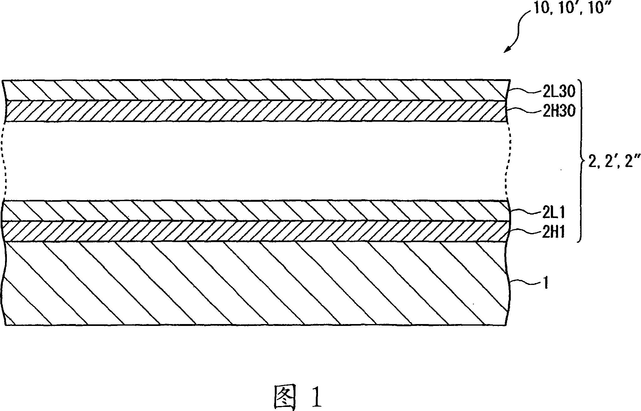
[0039] FIG. 1 is a cross-sectional view schematically showing the structure of an optical multilayer film filter 10 of the present invention. The optical multilayer film filter 10 is configured to include: a glass substrate 1 for transmitting light; and a multilayer inorganic thin film 2 formed on the upper surface of the glass substrate 1 .
[0040] The glass substrate 1 is white glass (refractive index n=1.52), and a glass substrate with a diameter of 30 mm and a thickness of 0.3 mm is used in this embodiment.
[0041] For the material of the inorganic thin film 2, the high refr...
Embodiment 8
[0101] Next, an electronic device configured including the optical multilayer film filter 10 of Examples 1 to 7 will be described. The present embodiment is an embodiment applied as an electronic device to, for example, an imaging device of a digital still camera that captures still images.
[0102] FIG. 6 is an explanatory diagram showing an example of the configuration of an electronic device according to the present invention, and shows a configuration example of the camera module 100 and the camera device 400 including the camera module 100 . The imaging module 100 shown in FIG. 6 is configured to include: an optical multilayer film filter 10, an optical low-pass filter 110, a CCD (charge-coupled device) 120 of an imaging element that electrically converts an optical image, and a device that drives the imaging element 120. The drive unit 130.
[0103] The optical multilayer film filter 10 is composed of a glass substrate 1 and an inorganic thin film 2 as described in an e...
PUM
| Property | Measurement | Unit |
|---|---|---|
| density | aaaaa | aaaaa |
| diameter | aaaaa | aaaaa |
| thickness | aaaaa | aaaaa |
Abstract
Description
Claims
Application Information
 - R&D
- Intellectual Property
- Life Sciences
- Materials
- Tech Scout
- Unparalleled Data Quality
- Higher Quality Content
- 60% Fewer Hallucinations
Browse by: Latest US Patents, China's latest patents, Technical Efficacy Thesaurus, Application Domain, Technology Topic, Popular Technical Reports.
© 2025 PatSnap. All rights reserved.Legal|Privacy policy|Modern Slavery Act Transparency Statement|Sitemap|About US| Contact US: help@patsnap.com


