Light irradiation apparatus, light irradiation method, crystallization apparatus, crystallization method, and semiconductor device

A light irradiation device and light irradiation technology, applied in semiconductor/solid-state device manufacturing, crystal growth, optical components, etc., can solve problems such as inconvenience, inability to generate crystal grains, and inability to generate light intensity distribution.

Inactive Publication Date: 2007-09-19
ADVANCED LCD TECH DEVMENT CENT
View PDF0 Cites 0 Cited by
  • Summary
  • Abstract
  • Description
  • Claims
  • Application Information

AI Technical Summary

Problems solved by technology

However, if the α value is set to a relatively large value (for example, 0.6 or more), wavelike fluctuations indicating light intensity are produced on the contour line, failing to produce the desired light intensity distribution
As a result, unevenness occurs in the growth of the crystal, and crystal grains having a desired shape cannot be produced, so that the electrical properties of the produced TFT fluctuate, which is inconvenient

Method used


Image

  • Light irradiation apparatus, light irradiation method, crystallization apparatus, crystallization method, and semiconductor device
  • Light irradiation apparatus, light irradiation method, crystallization apparatus, crystallization method, and semiconductor device
  • Light irradiation apparatus, light irradiation method, crystallization apparatus, crystallization method, and semiconductor device

Examples


Embodiment Construction

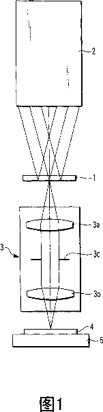
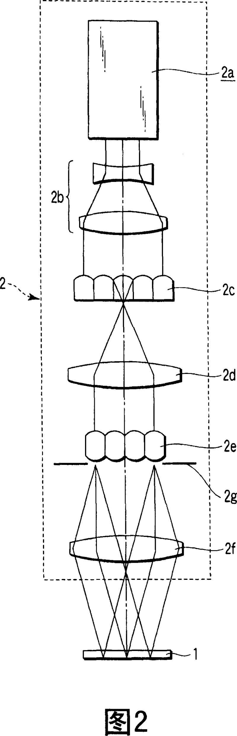
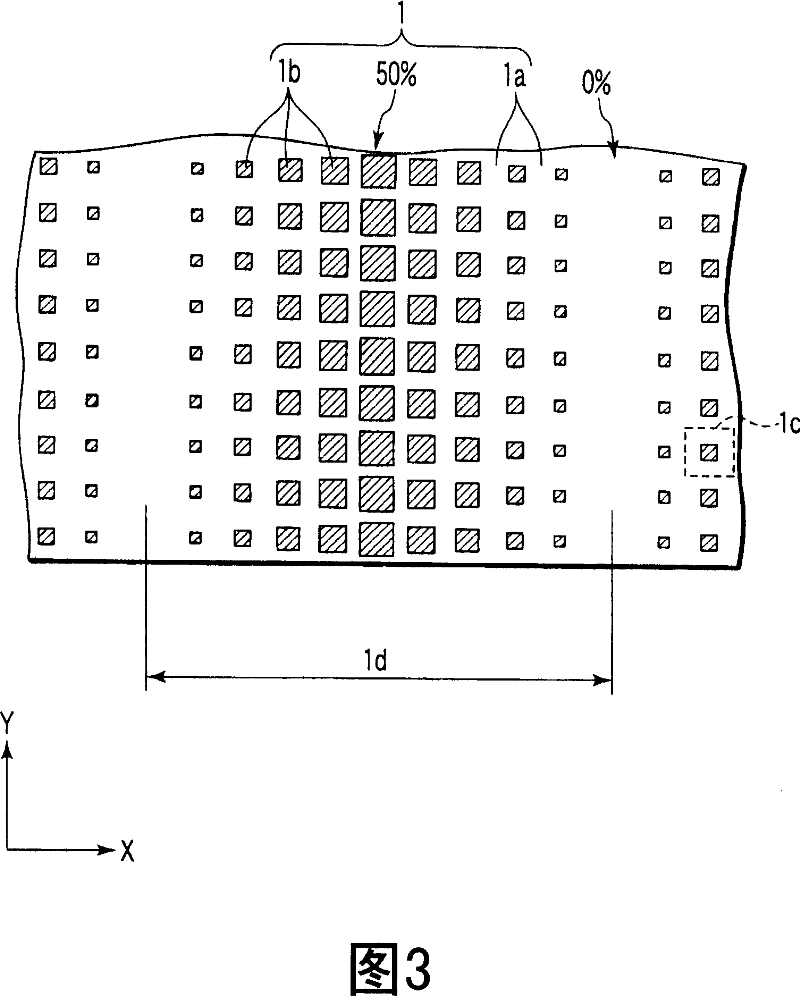
[0055] Embodiments according to the present invention are explained below with reference to the drawings. FIG. 1 is a schematic diagram illustrating a crystallization apparatus according to an embodiment of the present invention. FIG. 2 is a view schematically showing the internal structure of the lighting system of FIG. 1 . 1 and 2, the crystallization apparatus according to the present embodiment includes a light modulation element 1 such as a phase shifter, which modulates the phase of incident light (beam) to form light (beam) with a predetermined light intensity distribution, the illumination light modulation An illumination system 2 of the element 1, an image forming optical system 3, and a substrate pole 5 holding a processing target substrate 4 having a semiconductor film such as non-single crystal silicon.

[0056] The structure and function of the light modulation element 1 are explained later. The illumination system 2 includes a XeCl excimer laser (beam) source 2...


PUM

PropertyMeasurementUnit
wavelengthaaaaaaaaaa

Abstract

A light irradiation apparatus irradiates a target plane with light having a predetermined light intensity distribution. The apparatus includes a light modulation element having a light modulation pattern of a periodic structure represented by a primitive translation vector (a 1,a 2 ), an illumination system for illuminating the modulation element with the light, and an image forming optical system for forming the predetermined light intensity distribution obtained by the modulation pattern on the target plane. A shape of an exit pupil of the illumination system is similar to the Wigner-Seitz cell of a primitive reciprocal lattice vector (b 1,b 2 ) obtained from the primitive translation vector (a 1, a 2 ) by the following equations: b1=2pi(a2xa3) / (a1.(a2xa3)) and b2=2pi(a3xa1) / (a1.(a2xa3)) in which a 3 is a vector having an arbitrary size in a normal direction of a flat surface of the modulation pattern of the modulation element,''.'' is an inner product of the vector, and ''x'' is an outer product of the vector.

Description

technical field [0001] The present invention relates to a light irradiation device, a light irradiation method, a crystallization device, a crystallization method, and relates to, for example, irradiating a non-single crystal semiconductor film with a laser beam having a predetermined light intensity distribution to produce a crystallized semiconductor film. Background technique [0002] Thin film transistors (TFTs) and the like used for switching elements such as selecting display pixels of a liquid crystal display (LCD) are conventionally formed of amorphous silicon or polycrystalline silicon. It is well known that polysilicon has higher mobility of electrons or holes than amorphous silicon. [0003] Therefore, when the transistor is formed of polysilicon, the switching speed becomes faster, and the display response speed also becomes higher than the case where the transistor is formed of amorphous silicon. In addition, LSIs placed around devices, such as driver circuits ...

Claims


Application Information

Patent Timeline
Patent Type & Authority Applications(China)
IPC IPC(8): H01L21/00H01L21/20H01L21/268H01L21/336G02F1/01G02F1/35G02B27/00B23K26/06
CPCY10T117/10Y10T117/1008C30B13/24H01L21/02675C30B13/22H01L21/20
Inventor 谷口幸夫
Owner ADVANCED LCD TECH DEVMENT CENT
Why Eureka
Try Eureka