


Quick Research
Generate reliable direction feasibility study reports for your R&D in just a few steps.

Technical Q&A
Discover and master advanced knowledge NOW. Basics, ideas, possibilities, all at once.

Find Solutions
As an expert in R&D theories, this can generate solutions to your technical problems instantly.

Evaluate Feasibility
Analyze your overall solution with one click, know your potential R&D risks in advance.

Monitor Landscape
Get weekly tech updates, stay abreast of the latest tech innovations and key insights.
High breakdown voltage semiconductor integrated circuit device and dielectric separation type semiconductor device
A technology of integrated circuits and semiconductors, applied in the fields of semiconductor devices, semiconductor/solid-state device manufacturing, circuits, etc., can solve the problems of easy accumulation of impurities, difficult oxide films, and inability of semiconductor devices to function, to prevent displacement and achieve high reliability. , Improve the effect of insulation withstand voltage
- Summary
- Abstract
- Description
- Claims
- Application Information
AI Technical Summary
Problems solved by technology
Method used
Image


Examples
no. 1 approach
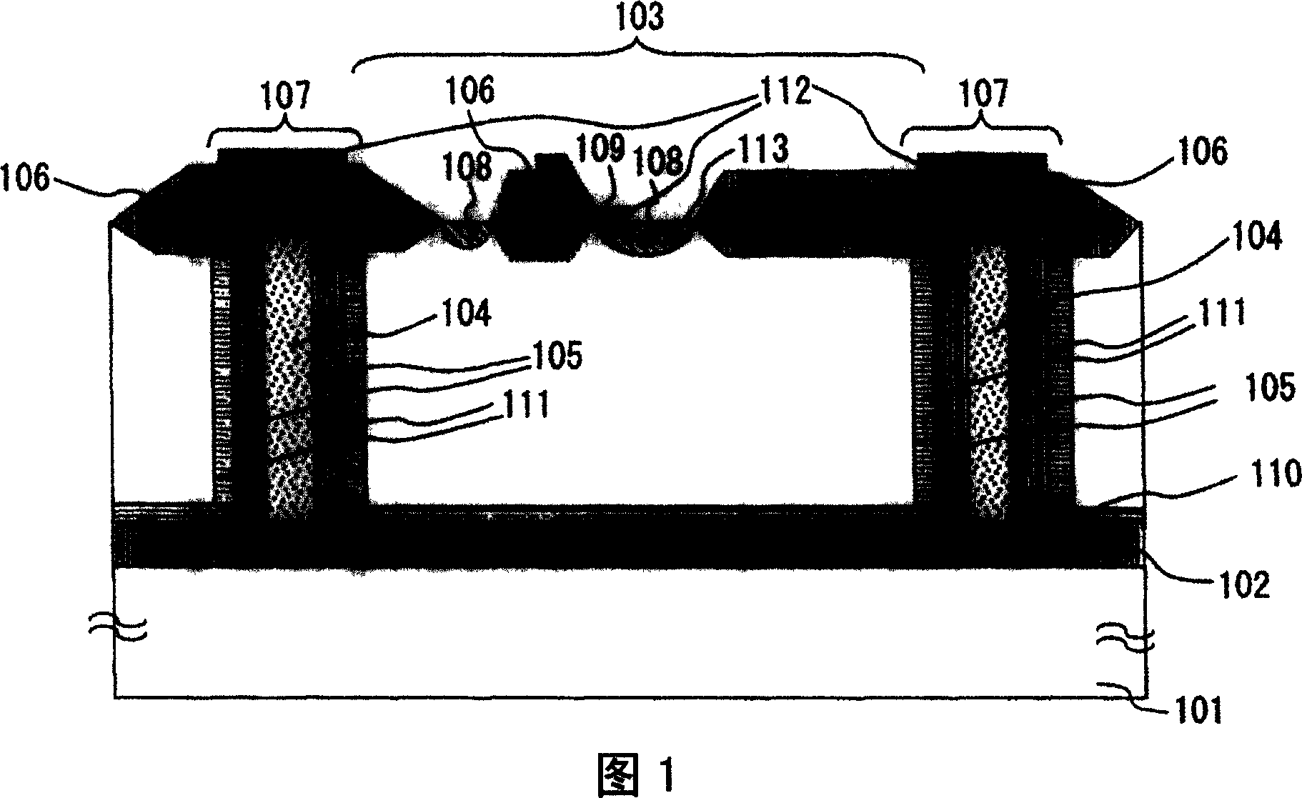
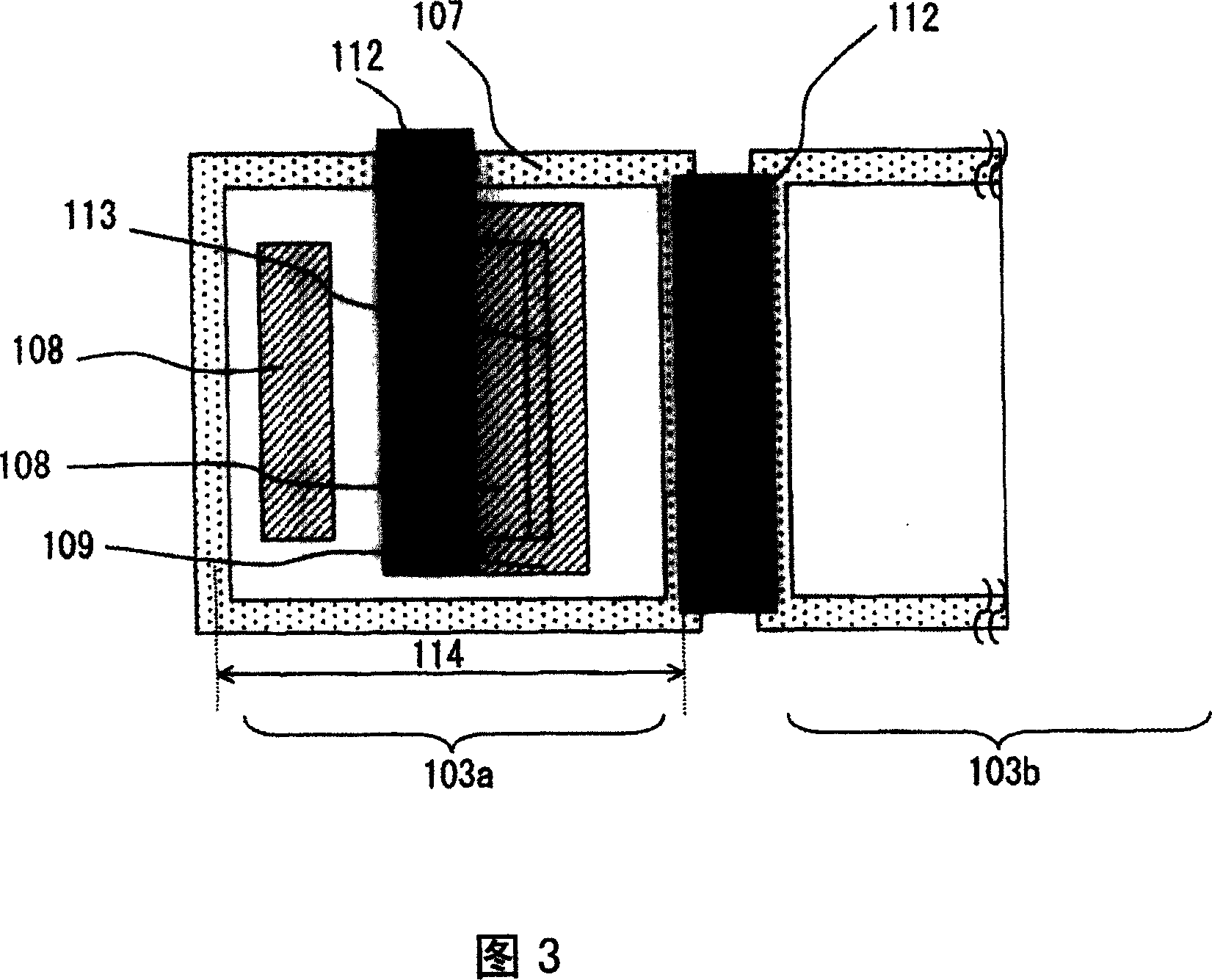
[0064] Hereinafter, embodiments of the present invention will be described with reference to the drawings. FIG. 1 shows a cross-sectional view of a semiconductor integrated circuit device according to this embodiment. In Fig. 1, the symbol 101 represents a silicon support substrate, 102 is a buried oxide film, 103 is an element region, 104 is a buried polysilicon film, 105 is a side oxide film, 106 is a surface oxide film, 107 is a trench, and 108 is n + Dope (dope) region, 109 is p-doped region, 110 is buried n + Doped region, 111 is the side n + Doped region, 112 is polysilicon wiring, 113 is p + doped region. In addition, FIG. 3 shows a plan view of the semiconductor integrated circuit device of the present embodiment. Two element formation regions 103a and 103b are formed adjacent to each other. Polysilicon wiring 112 is formed to straddle trench 107 . Symbol 114 in FIG. 3 represents the first side of the trench. In this embodiment, the structure is adopted: thermal...
no. 2 approach
[0073] FIG. 8 shows a cross-sectional view of the semiconductor integrated circuit device of this embodiment. In this embodiment, a plurality of trenches 107 are formed in the isolation region. In FIG. 8 , the case surrounded by two grooves is illustrated. Usually, although it is designed in such a way that the rated insulation withstand voltage can be obtained with one groove, if multiple grooves 107 are provided, it is possible to greatly reduce the disadvantages generated inside the grooves 107 during the processing process. bad rate.
[0074] FIG. 9 shows changes in the defect rate when the number of grooves is changed. The defective rate is the ratio of the number of measured units whose dielectric withstand voltage dropped by 30% or more based on the average value when measuring the dielectric withstand voltage of 2,000 different integrated circuit devices. From this result, it can be seen that when a plurality of trenches are provided as in the semiconductor integrat...
no. 3 approach
[0076] In the semiconductor integrated circuit device of this embodiment, the thickness of the side oxide film 105 formed in the trench is reduced. If the thickness of the side oxide film 105 is reduced, the stress generated at the interface between silicon oxide and silicon during formation of the side oxide film can be reduced, thereby reducing the defect rate due to defects.
[0077] FIG. 10 shows the relationship between the breakdown voltage ratio and the value obtained by dividing the thickness of the buried oxide film 102 by the thickness of the oxide film 105 on the inner surface of the trench. The defective rate is the ratio of the number of measurement points whose dielectric withstand voltage drops by 30% or more based on the average value when measuring the dielectric withstand voltage of 1000 different integrated circuit devices. From this result, it can be seen that when the value obtained by dividing the film thickness of the buried oxide film 102 by the film th...
PUM
 Abstract
Description
Claims
Application Information
 - R&D Engineer
- R&D Manager
- IP Professional
- Industry Leading Data Capabilities
- Powerful AI technology
- Patent DNA Extraction
Browse by: Latest US Patents, China's latest patents, Technical Efficacy Thesaurus, Application Domain, Technology Topic, Popular Technical Reports.
© 2024 PatSnap. All rights reserved.Legal|Privacy policy|Modern Slavery Act Transparency Statement|Sitemap|About US| Contact US: help@patsnap.com