TFT LCD array substrate structure and method for forming non-comformal insulation film and use
A technology of insulating thin film and thin film, which is applied in the direction of nonlinear optics, instruments, semiconductor devices, etc., can solve problems such as failure of thin film transistor devices and dead pixels of liquid crystal display devices, so as to reduce invisible defects and dead pixels of displays, and reduce development costs and cost of use, the effect of reducing the probability of occurrence
- Summary
- Abstract
- Description
- Claims
- Application Information
AI Technical Summary
Problems solved by technology
Method used
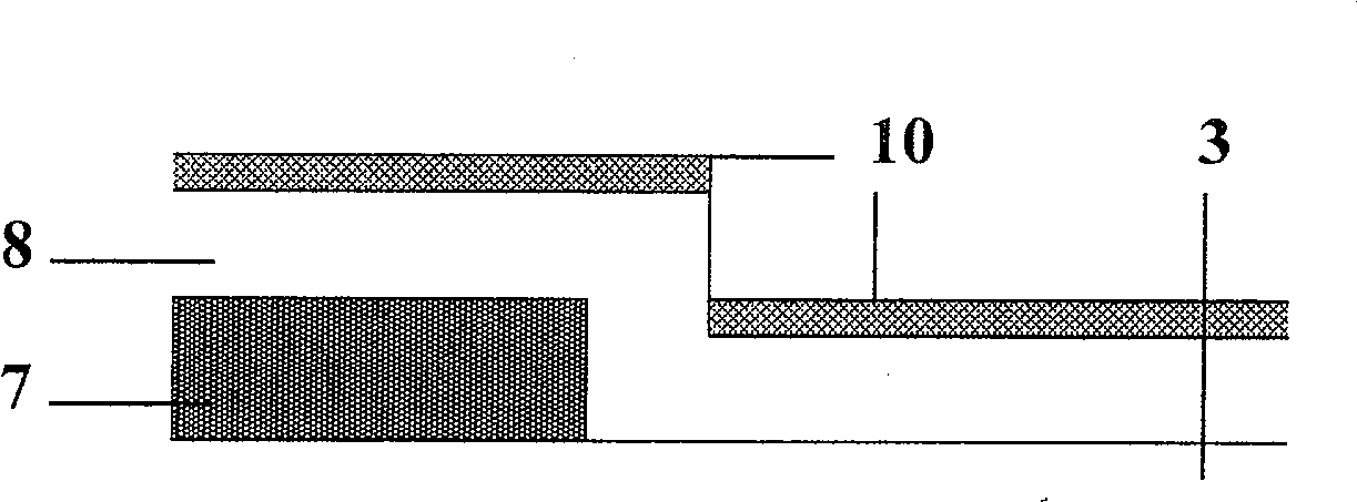
Image

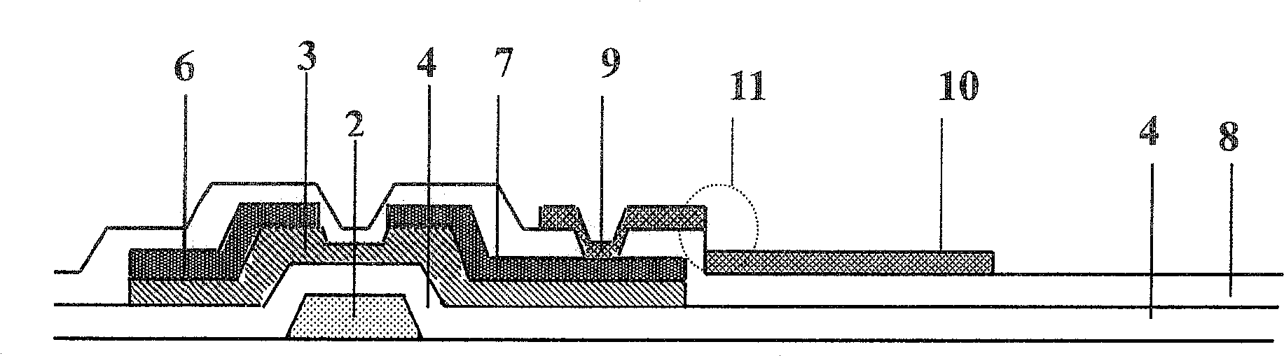
Examples
Embodiment 1
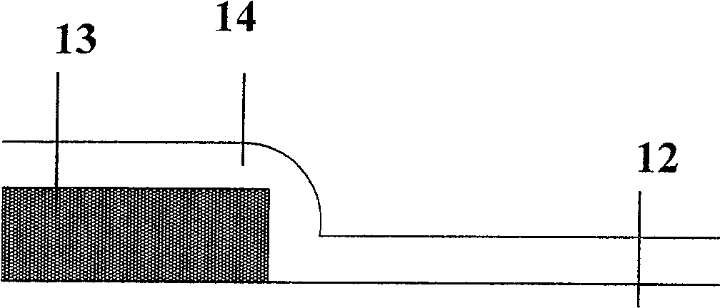
[0048] First, if image 3 As shown, a substrate 12 on which a conductive film 13 (which may be a gate electrode film or a source-drain electrode film, etc.) has been formed is provided.
[0049] Then, the aforementioned substrate 12 is placed in the plasma-enhanced chemical vapor deposition equipment. In addition to passing reactive gases such as silane, ammonia and nitrogen to the plasma-enhanced chemical vapor deposition equipment for depositing insulating films, the inert gases such as argon, Or helium, or a mixed gas of helium and hydrogen, the film is etched while the film is deposited to form a non-conformal insulating film 14 . For example, the inert gas argon is fed into the plasma, and the generated argon ions are accelerated to the surface of the substrate under the action of an electric field, and bombard the surface film, resulting in film etching while depositing the film. Such as image 3 As shown, the insulating film 14 above the conductive film 13 forms a non...
Embodiment 2
[0051] Figure 4a to Figure 4d The specific fabrication process of this embodiment is given.
[0052] Firstly, a substrate 12 on which a conductive thin film 13 (may be a gate line and a gate electrode or a source-drain electrode, etc.) has been formed is provided.
[0053] Subsequently, the substrate 12 is placed in the plasma-enhanced chemical vapor deposition equipment, and reactive gases such as silane, ammonia, and nitrogen are introduced into the reaction chamber. After a certain period of time, a first layer of insulating film 14a with a certain thickness is deposited to stop the reaction. Gas access. Due to the inherent conformal properties of plasma-enhanced chemical vapor deposition, the first insulating film 14a is formed Figure 4a The vertical steps shown.
[0054] Next, the inert gas is fed into the plasma-enhanced chemical vapor deposition equipment, and the inert gas plasma is generated under a certain power and pressure, and the inert gas ions bombard the s...
PUM
| Property | Measurement | Unit |
|---|---|---|
| thickness | aaaaa | aaaaa |
Abstract
Description
Claims
Application Information
 - Generate Ideas
- Intellectual Property
- Life Sciences
- Materials
- Tech Scout
- Unparalleled Data Quality
- Higher Quality Content
- 60% Fewer Hallucinations
Browse by: Latest US Patents, China's latest patents, Technical Efficacy Thesaurus, Application Domain, Technology Topic, Popular Technical Reports.
© 2025 PatSnap. All rights reserved.Legal|Privacy policy|Modern Slavery Act Transparency Statement|Sitemap|About US| Contact US: help@patsnap.com