Nonvolatile semiconductor memory device and read method
A storage device, non-volatile technology, applied in information storage, static memory, read-only memory, etc.
- Summary
- Abstract
- Description
- Claims
- Application Information
AI Technical Summary
Problems solved by technology
Method used
Image

Examples
no. 1 Embodiment approach
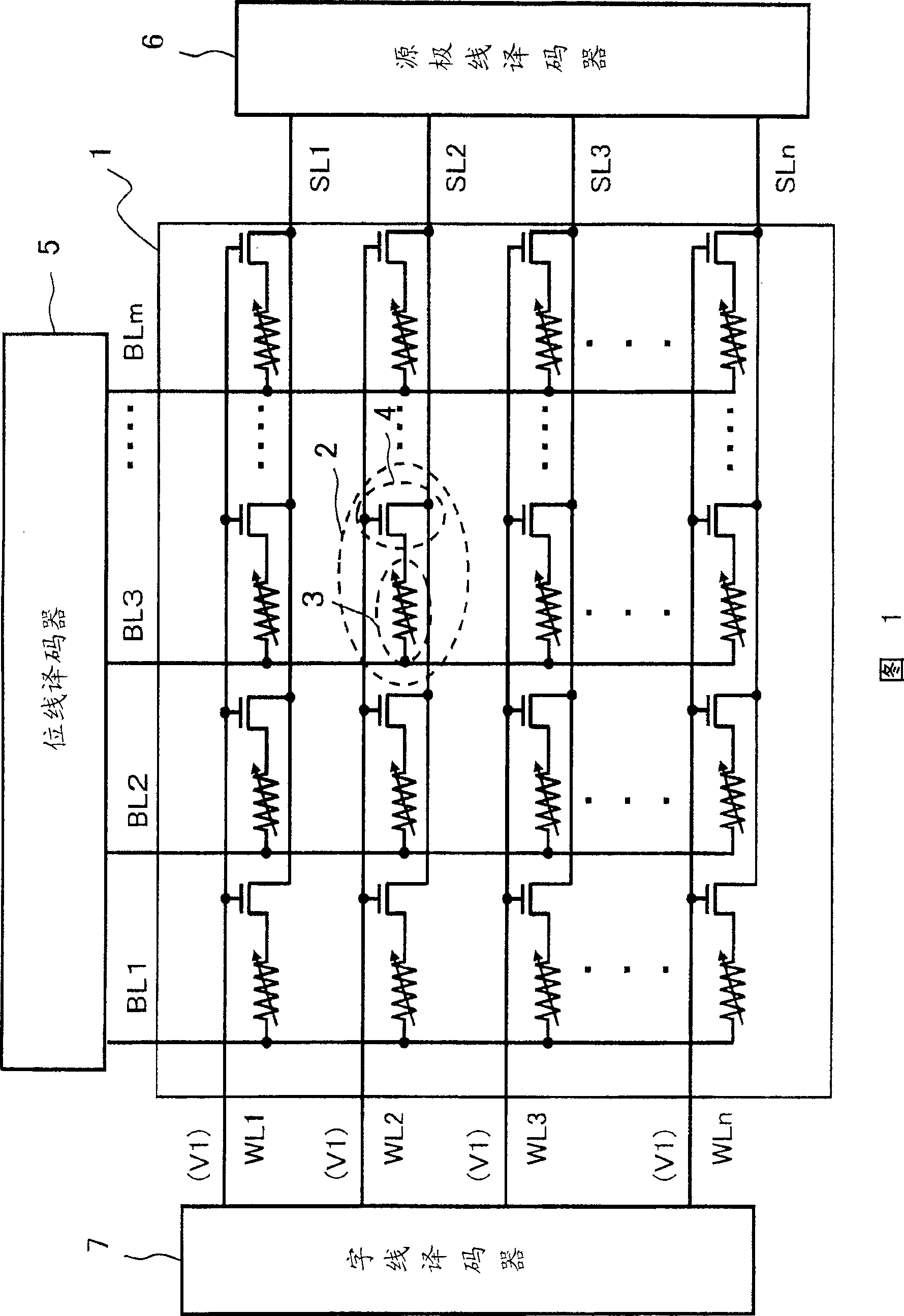
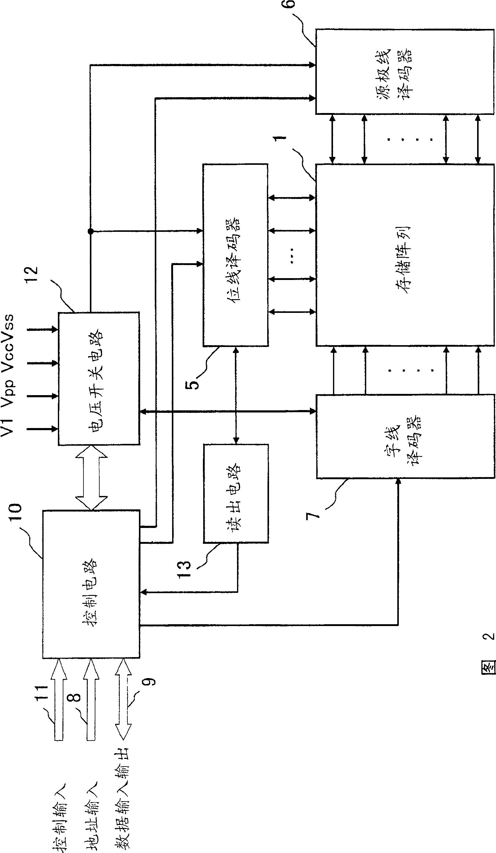
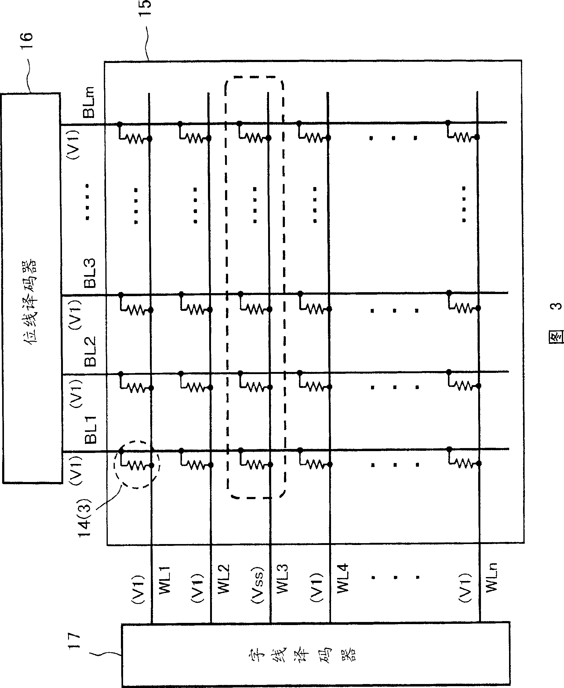
[0076]Fig. 8 shows an example of the configuration of the device of the present invention. In addition, in FIG. 8 , the parts common to those of the conventional nonvolatile semiconductor memory device will be described with common reference numerals. As shown in FIG. 8, the device of the present invention has a bit line decoder 16, a word line decoder 17, and a voltage switch circuit 22a around a memory cell array 15 in which 1R type memory cells (not shown) are arranged in a matrix. , the readout circuit 23 and the control circuit 20a. Basically, the configuration is the same as that of a conventional nonvolatile semiconductor memory device having a memory cell array of 1R type memory cells shown in FIG. 5 . The difference from the conventional nonvolatile semiconductor memory device of FIG. 5 lies in the voltage applied from the voltage switch circuit 22a to the memory cell array 15 and its timing operation and the operation of the control circuit 20a for controlling the o...
Embodiment 1
[0083] First, referring to Figure 9 and Figure 10 In the first embodiment, in order to perform a data read operation, a read voltage is applied to a selected memory cell, and then a dummy read voltage for suppressing a change in resistance of the selected memory cell is applied.
[0084] In Figure 9 and Figure 10 2 shows the sequence of applying voltages to each part during an example data read operation of the memory cell array 15 of the device of the present invention.
[0085] First, when reading the data of the selected memory cell, the selected word line connected to the selected memory cell is maintained at the ground potential Vss, and the read period Tr is applied to the other non-selected word lines and all the bit lines. Voltage V1. In the read period Tr, since a voltage difference of the read voltage V1 is generated between the selected word line and the selected bit line, the variable resistance element of the selected memory cell flows a read current correspon...
Embodiment 2
[0089] Second, referring to Figure 9 and Figure 11 In the second embodiment, in order to perform a data read operation, a read voltage is applied to a selected memory cell, and then a dummy read voltage for suppressing a change in resistance of the selected memory cell is applied. At this time, a voltage V2 having a voltage value twice the voltage V1 is supplied to the voltage switch circuit 22a of the device of the present invention shown in FIG. 8 .
[0090] In Figure 9 and Figure 11 2 shows the sequence of applying voltages to each part during an example data read operation of the memory cell array 15 of the device of the present invention.
[0091] First, when reading the data of the selected memory cell, the selected word line connected to the selected memory cell is maintained at the ground potential Vss, and the read period Tr is applied to the other non-selected word lines and all the bit lines. Voltage V1. In the read period Tr, since a voltage difference of the ...
PUM
 Abstract
Description
Claims
Application Information
 - R&D
- Intellectual Property
- Life Sciences
- Materials
- Tech Scout
- Unparalleled Data Quality
- Higher Quality Content
- 60% Fewer Hallucinations
Browse by: Latest US Patents, China's latest patents, Technical Efficacy Thesaurus, Application Domain, Technology Topic, Popular Technical Reports.
© 2025 PatSnap. All rights reserved.Legal|Privacy policy|Modern Slavery Act Transparency Statement|Sitemap|About US| Contact US: help@patsnap.com