Method for improving emission property of deposited carbon nano-tube thin film electronic field by electrophorisis method
A technology of emission performance and carbon deposition, applied in the manufacture of discharge tubes/lamps, electrophoretic plating, nanotechnology, etc., can solve problems such as restricting the practical application of electrophoresis, easy peeling of carbon nanotube films, unstable field emission current, etc. , to enhance the resistance to ion bombardment, eliminate the interface barrier, and improve the emission stability.
- Summary
- Abstract
- Description
- Claims
- Application Information
AI Technical Summary
Problems solved by technology
Method used
Image

Examples
Embodiment 1
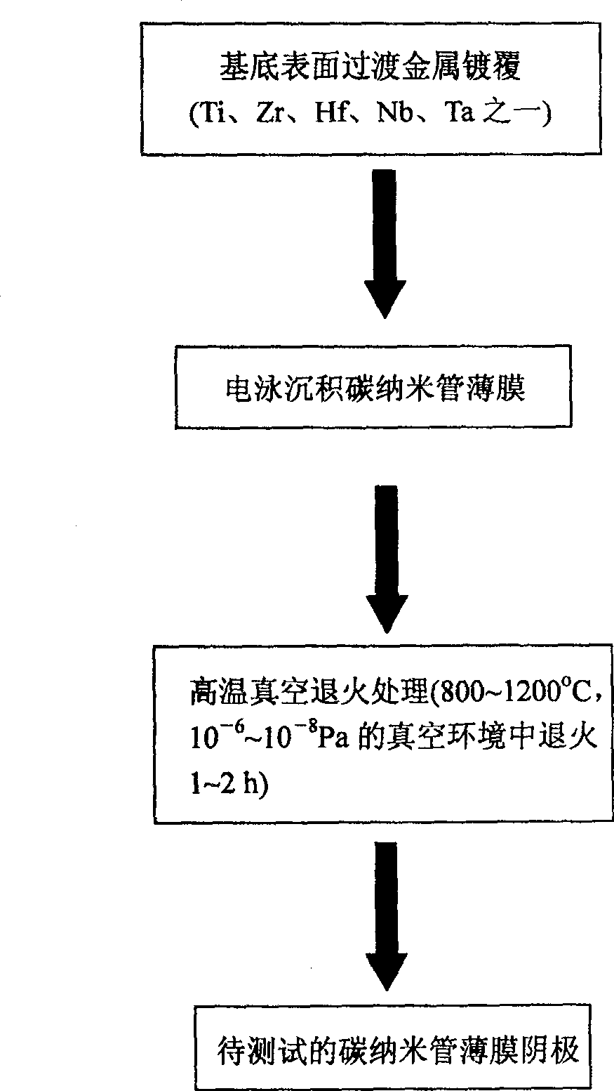
[0023] (1) Coating a transition metal thin film on the base material by radio frequency magnetron sputtering coating method. The transition metal is Ti, and the base material is p-type (100) Si sheet. The specific sputtering coating conditions are as follows: adjust the sputtering power to 80W so that the deposition rate is 0.22nm / s, the sputtering time is 15min, and the sputtering vacuum is 3×10 -4 Pa, the thickness of the plated Ti film is 200nm.
[0024] (2) The Si substrate coated with Ti film was used as the cathode, and the carbon nanotube film was deposited by electrophoresis, and the film thickness was 30 μm. The electrophoretic fluid consists of 0.3g carbon nanotubes and 0.2g Mg(NO 3 ) 2 ·6H 2 O is dispersed in 200ml of isopropanol, ultrasonically oscillated for 2 hours, and then settled for 1 hour to obtain it; the process conditions during electrophoresis are: electrophoresis voltage 100V, electrophoresis time 2min, distance between cathode and anode 2cm; the an...
Embodiment 2
[0027] (1) Coating a transition metal thin film on the base material by vacuum evaporation coating method. The transition metal is Ta, and the base material is p-type (100) Si sheet. The process conditions are: the deposition rate is 0.4nm / s, and the deposition vacuum is 6×10⁻⁵ Pa, deposition time 4min, sputtering vacuum 3×10 -4 Pa, the thickness of the plated Ta film is 100nm.
[0028] (2) The Si substrate coated with Ta film was used as the cathode, and the carbon nanotube film was deposited by electrophoresis, and the film thickness was 30 μm. The electrophoretic fluid consists of 0.3g carbon nanotubes and 0.2g Mg(NO 3 ) 2 ·6H 2 O is dispersed in 200ml isopropanol, ultrasonically oscillated for 2 hours, and then settled for 1 hour; the anode used is a platinum electrode; the process conditions during electrophoresis are: electrophoresis voltage 60V, electrophoresis time 5min, distance between cathode and anode 3cm; The nanotubes are multi-walled carbon nanotubes prepar...
Embodiment 3
[0031] (1) Coating a transition metal thin film on the base material by radio frequency magnetron sputtering coating method. The transition metal is Hf, and the base material is p-type (100) Si sheet. The process conditions are: adjust the sputtering power to 200W so that the deposition rate is 0.8nm / s, the sputtering time is 8min, and the sputtering vacuum is 3×10 -4 Pa, the thickness of the plated Hf film is 400nm.
[0032] (2) The Si substrate coated with Ta film was used as the cathode, and the carbon nanotube film was deposited by electrophoresis, and the film thickness was 25 μm. The electrophoretic fluid consists of 0.3g carbon nanotubes and 0.2g Mg(NO 3 ) 2 ·6H 2 O is dispersed in 200ml of isopropanol, ultrasonically oscillated for 2 hours, and then settled for 1 hour; the anode used is a stainless steel electrode; the process conditions during electrophoresis are: electrophoresis voltage 60V, electrophoresis time 5min, distance between cathode and anode 3cm; The ...
PUM
| Property | Measurement | Unit |
|---|---|---|
| thickness | aaaaa | aaaaa |
| diameter | aaaaa | aaaaa |
| diameter | aaaaa | aaaaa |
Abstract
Description
Claims
Application Information
 - R&D
- Intellectual Property
- Life Sciences
- Materials
- Tech Scout
- Unparalleled Data Quality
- Higher Quality Content
- 60% Fewer Hallucinations
Browse by: Latest US Patents, China's latest patents, Technical Efficacy Thesaurus, Application Domain, Technology Topic, Popular Technical Reports.
© 2025 PatSnap. All rights reserved.Legal|Privacy policy|Modern Slavery Act Transparency Statement|Sitemap|About US| Contact US: help@patsnap.com