Silicon photoelectric probe compatible with deep submicron radio frequency technology

A deep submicron, silicon photoelectric technology, applied in photometry, electro-solid devices, optical radiation measurement, etc., can solve the problems of limited fiber coupling range, large parasitic capacitance, etc., to achieve high yield, improved performance, reliability good effect

Inactive Publication Date: 2008-11-12
TIANJIN UNIV
View PDF4 Cites 0 Cited by
  • Summary
  • Abstract
  • Description
  • Claims
  • Application Information

AI Technical Summary

Problems solved by technology

Hybrid integration makes the surface near the detector have protruding bonding wires, which limits the active range of fiber coupling, and usually the area of ​​a bonding pad is 100×100μm 2 , resulting in a large parasitic capacitance

Method used


Image

  • Silicon photoelectric probe compatible with deep submicron radio frequency technology
  • Silicon photoelectric probe compatible with deep submicron radio frequency technology

Examples


Embodiment Construction

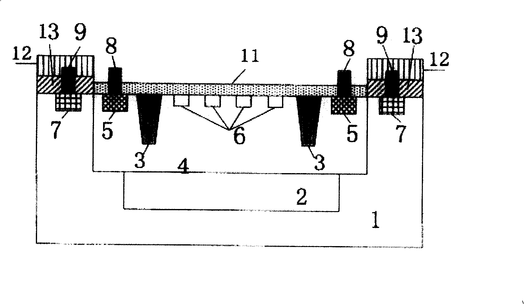
[0015] The present invention is achieved by the following methods: figure 1 Shows the layout structure of the photodetector for fabrication on a deep submicron RF__CMOS process, figure 2 A longitudinal cross-sectional structure diagram of the photodetector is shown, mainly showing the longitudinal dimension of the photodetector.

[0016] p - type semiconductor substrate 1, deep n-type well 2, the deep n-type well 2 is fabricated in the substrate 1; n-type well 4, the n-type well 4 is fabricated on the substrate 1; shallow trench isolation region 3, the Shallow trench isolation region 3 is fabricated in n-type well 4; four interdigitated P + Type diffusion region 6, the four interdigitated P+ type diffusion regions 6 are arranged on the n-type well 4; P + Type guard ring 7, the P + type guard ring 7 is fabricated on the substrate 1 and around the n-type well 4; the anti-reflection coating layer 11 is deposited on four interdigitated P + Type diffusion region 6 above; by t...


PUM


Abstract

The invention discloses a high-speed silicon photoelectric detector compatible with deep submicron radio-frequency_compensatory metal oxide semiconductor (RF_COMS) technique, and it adopts a technical project: there is a deep n-type trap arranged in a p-type semiconductor substrate, a shallow channel is arranged in the n-type trap, four interdigital p+-type diffusion regions are arranged on the n-type trap; the diffusion regions are provided with antireflecting films, the p+-type diffusion regions and the n-type trap compose a p-n junction of photoelectric diode and the n-type trap and the P+-type protective rings compose a screening diode. It can be applied in many fields like CD-ROMs, digital video CDs (DVDs), and digital systems.

Description

technical field [0001] The invention relates to a photodetector structure and manufacturing method, in particular to a silicon-based photodetector structure fully compatible with deep submicron radio frequency standard complementary metal oxide semiconductor (RF_CMOS) technology. Background technique [0002] At present, the mainstream receivers are compound photodetectors, which are mixed and integrated with silicon-based receiver ASICs by wire bonding (WIREBONDING). Hybrid integration makes the surface near the detector have protruding bonding wires, which limits the active range of fiber coupling, and usually the area of ​​a bonding pad is 100×100μm 2 , resulting in a large parasitic capacitance. The invention not only realizes monolithic integration of full siliconization of the optical receiver, but also realizes full compatibility with high-speed CMOS circuits, such as radio frequency integrated circuits (RFIC). This makes the function of the optical receiver more fl...

Claims


Application Information

Patent Timeline
Patent Type & Authority Patents(China)
IPC IPC(8): H01L27/14H01L31/10G01J1/02
Inventor 毛陆虹李炜陈弘达陈永权张晓潇
Owner TIANJIN UNIV
Why Eureka
Try Eureka