Semiconductor device, method for manufacturing same, and power converter using such semiconductor device

A technology of semiconductors and light-emitting semiconductors, applied in semiconductor devices, semiconductor/solid-state device components, circuits, etc., can solve problems such as large constant loss, large total loss, and difficult power semiconductor devices

Inactive Publication Date: 2008-09-03
THE KANSAI ELECTRIC POWER CO
View PDF6 Cites 0 Cited by
  • Summary
  • Abstract
  • Description
  • Claims
  • Application Information

AI Technical Summary

Problems solved by technology

Therefore, since the constant loss of a semiconductor device of SiC is very large, the total loss is larger than that of a semiconductor device of Si
As mentioned above, it is difficult to realize SiC power semiconductor devices with low loss and high current control in the prior art

Method used


Image

  • Semiconductor device, method for manufacturing same, and power converter using such semiconductor device
  • Semiconductor device, method for manufacturing same, and power converter using such semiconductor device
  • Semiconductor device, method for manufacturing same, and power converter using such semiconductor device

Examples


no. 1 example

[0051] The semiconductor device according to the first embodiment of the present invention is a SiC (silicon carbide) pn diode device 19 with a withstand voltage of 8.5 kV, which will be described below with reference to FIG. 1 .

[0052] FIG. 1 is a cross-sectional view of a SiC-pn diode device 19 according to a first embodiment of the present invention. In FIG. 1, the SiC pn diode element 13 is a 4-layer hexagonal element, and a low impurity concentration n-type SiC with a thickness of approximately 95 μm is formed on the cathode region 1 of a high impurity concentration n-type SiC with a thickness of approximately 300 μm. Drift layer 2. A cathode metal electrode 7 is formed below the cathode region 1 . An anode region 3 of p-type SiC constituting a main bond with the drift layer 2 is formed in the central region of the drift layer 2 . An electric field relaxation region 4 of p-type SiC is formed around the anode region 3 . An anode metal electrode 6 is formed on the anod...

no. 2 example

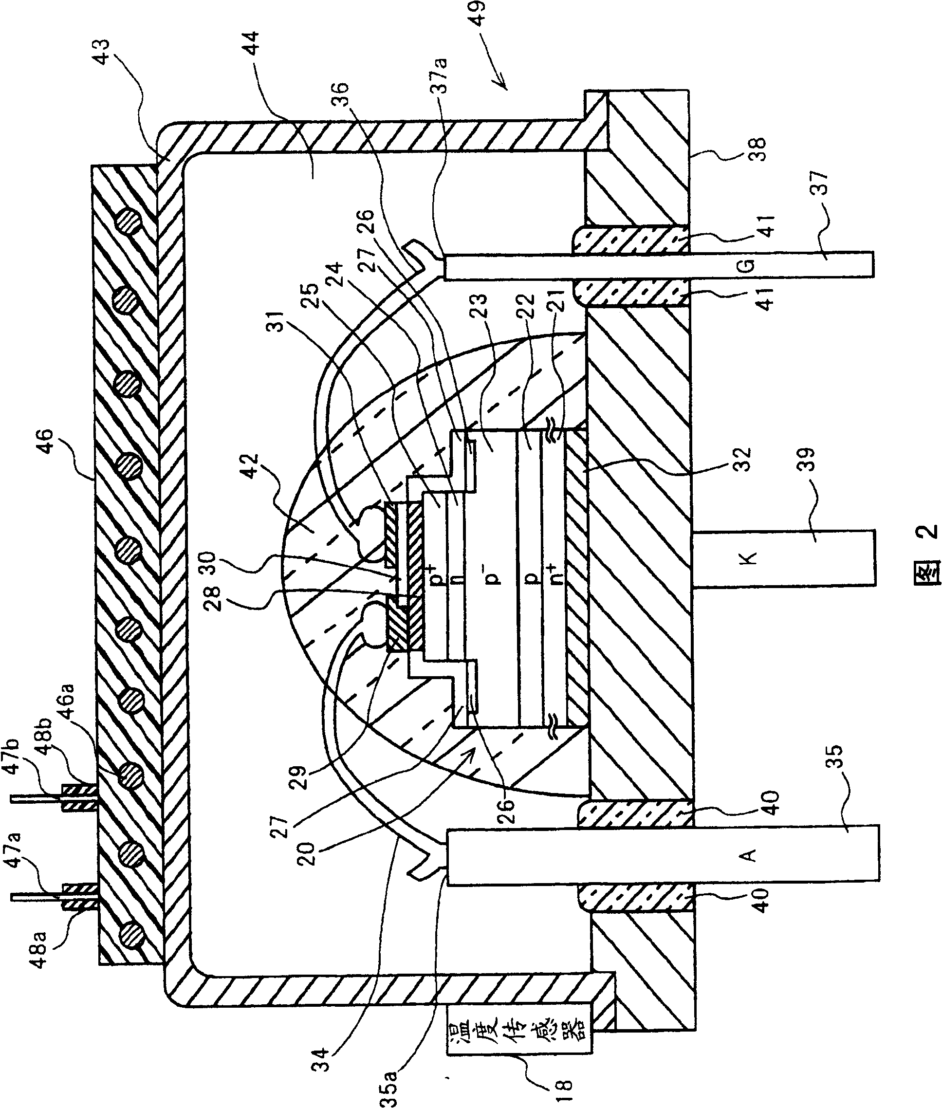
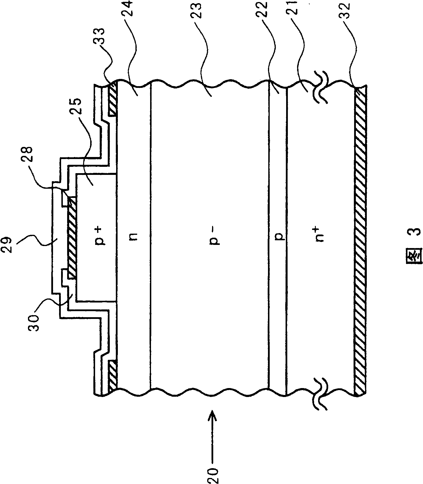
[0063] The semiconductor device according to the second embodiment of the present invention is a SiC-GTO thyristor (Gate Turn-Off Thyristor) device 49 with a withstand voltage of 5 kV, and FIG. 2 shows its cross-sectional view. FIG. 3 is a cross-sectional view showing a unit obtained by cutting the GTO thyristor element 20 in FIG. 2 along a plane perpendicular to the paper. In an actual element, a plurality of units shown in FIG. 3 are connected in the left-right direction of the drawing. In addition, in FIG. 2, a plurality of units shown in FIG. 3 are connected in a direction perpendicular to the paper surface of the drawing. In FIGS. 2 and 3 , a p-type SiC buffer layer 22 having a thickness of about 3 μm is provided on a high impurity concentration n-type SiC cathode region 21 having a thickness of about 320 μm. A cathode electrode 32 is arranged below the cathode region 21 . A base layer 23 of p-type SiC having a thickness of about 60 μm and a low impurity concentration i...

no. 3 example

[0076] A semiconductor device according to a third embodiment of the present invention is an optically coupled wide-gap power semiconductor device, and FIG. 4 shows a cross-sectional view thereof. In the figure, a GaN (gallium nitride)-GTO thyristor element 51 with a withstand voltage of 3 kV and a current capacity of 160 A is used as a main power semiconductor element having a light emitting function. A SiC photodiode 52 is used as a light receiving element. A SiC photodiode 52 is provided in the same package facing the GaN-GTO thyristor element 51 .

[0077] In the GaN-GTO thyristor element 51 shown in FIG. 4 , a p-base of p-type GaN with a thickness of about 35 μm and a low impurity concentration is provided on the cathode region 51 a of n-type GaN with a thickness of about 250 μm and a high impurity concentration. polar region 53 . An n-base region 54 of high impurity concentration n-type GaN having a thickness of about 1.7 μm is formed in the central region of the p-bas...


PUM


Abstract

The temperature of a bipolar semiconductor element using a wide-gap semiconductor is raised using heating means, such as a heater, to obtain a power semiconductor device being large in controllable current and low in loss. The temperature is set at a temperature higher than the temperature at which the decrement of the steady loss of the wide-gap bipolar semiconductor element corresponding to the decrement of the built-in voltage lowering depending on the temperature rising of the wide-gap bipolar semiconductor element is larger than the increment of the steady loss corresponding to the increment of the ON resistance increasing depending on the temperature rising.

Description

technical field [0001] The present invention relates to a power semiconductor device having a large controllable current (maximum current capable of on / off control during energization), and a power conversion device using the power semiconductor device. Background technique [0002] Power semiconductor devices used in power devices that handle high voltage and high current require low power loss, large controllable current, and high reliability. Examples of conventional power semiconductor devices that can control a large current and have a large power capacity include silicon (Si) insulated gate bipolar transistors (IGBTs) and self-excited thyristors. The so-called self-excited thyristor is a thyristor capable of being on / off controlled by a gate control signal. Known are gate turn-off thyristors (GTO thyristors), electrostatic induction thyristors, MOS thyristors, and the like. In addition, as other power semiconductor devices, diodes having a pn junction, that is, pn ju...

Claims


Application Information

Patent Timeline
Patent Type & Authority Patents(China)
IPC IPC(8): H01L23/34H01L29/861H01L29/74H01L29/20H01L29/24H01L29/744
CPCH01L2924/01002H01L2924/19107H01L2224/73265H01L23/34H01L24/45H01L2224/48137H01L2924/01015H01L2224/48091H01L24/05H01L2924/01004H01L24/48H01L25/072H01L2224/45015H01L2924/01005H01L2924/01013H01L2224/45144H01L24/03H01L2924/15312H01L24/49H01L2224/4903H01L2224/48599H01L29/1608H01L29/744H01L2924/10157H01L2924/0105H01L2924/05042H01L29/8613H01L2224/04042H01L2924/01031H01L2924/01006H01L23/045H01L2924/3025H01L2924/13055H01L2924/20758H01L29/2003H01L2924/01079H01L2924/01074H01L2224/4823H01L2224/32245H01L2924/01014H01L2224/8592H01L2224/49111H01L2924/01082H01L2224/05599H01L23/345H01L2924/01007H01L2924/014H01L2924/01023H01L2924/16152H01L2224/05556H01L2224/49051H01L2224/48465H01L29/0619H01L2224/48227H01L2224/85399H01L2924/01033H01L2924/00014H01L2924/1301H01L2924/12032H01L2924/1305H01L2924/12036H01L2924/12041H01L2924/12043H01L2924/181H01L2924/00H01L2924/00012
Inventor 菅原良孝
Owner THE KANSAI ELECTRIC POWER CO
Why Eureka
Try Eureka