Method for preparing glass waveguide by single-side molten salt electric field assistant ion exchange
An ion exchange and electric field assisted technology, applied in the direction of optical waveguide and light guide, can solve the problems of metal film 8 corrosion, metal film 8 detachment, ion exchange cannot be performed normally, etc., and achieve the effect of reducing damage
- Summary
- Abstract
- Description
- Claims
- Application Information
AI Technical Summary
Problems solved by technology
Method used
Image
Examples
Embodiment 1
[0029] Embodiment 1: A buried waveguide is fabricated by using a low-temperature diffusion process.
[0030] (1) Doped with rare earth ions Er 3+ and Yb 3+Evaporate (or sputter) a layer of Al with a thickness of 80-200nm on the upper surface of the phosphate glass substrate, and make a strip-shaped diffusion window with a width of 4-12 μm on the submersion through photolithography and wet etching processes;
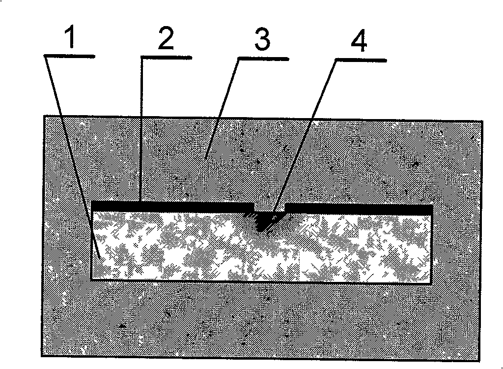
[0031] (2) Then put the masked glass substrate into an AgNO 3 with NaNO 3 and KNO 3 The ion exchange is carried out in the mixed molten salt, the ion exchange temperature is 280 ° C, the ion exchange time is 30 minutes, the Ag in the molten salt + The ion diffusion region 4 on the glass surface is formed in the glass substrate 1 through thermal diffusion, forming the core of the surface optical waveguide;
[0032] (3) the Al film on the surface of the glass substrate is made of H 3 PO 4 Corrosive solution removal;
[0033] (4) Evaporate (or sputter) a layer of Al ...
Embodiment 2
[0036] Embodiment 2: A buried waveguide is manufactured by a medium-temperature diffusion process.
[0037] (1) Evaporate (or sputter) a layer of Gr-Au with a thickness of 80-200 nm on the upper surface of the borate glass substrate, and make a layer of Gr-Au with a width of 4-12 μm on the submerged surface by photolithography and wet etching. Striped diffusion window;
[0038] (2) Then put the masked glass substrate into an AgNO 3 with NaNO 3 and KNO 3 The ion exchange is carried out in the mixed molten salt, the ion exchange temperature is 340 ° C, the ion exchange time is 10 minutes, the Ag in the molten salt + The ion diffusion area on the glass surface is formed in the glass substrate through thermal diffusion, forming the core of the surface optical waveguide;
[0039] (3) the Gr-Au film on the surface of the glass substrate is removed by a special standard Gr-Au etching solution for the microelectronics process;
[0040] (4) Evaporate (or sputter) a layer of Al wit...
Embodiment 3
[0042] Embodiment 3: A buried waveguide is fabricated by using a high temperature diffusion process.
[0043] (1) Evaporate (or sputter) a layer of Ag with a thickness of 80-200nm on the upper surface of the silicate glass substrate, and make strips with a width of 4-12μm on the submersion by photolithography and wet etching processes Diffusion window;
[0044] (2) Then put the masked glass substrate into an AgNO 3 with NaNO 3 and KNO 3 The ion exchange is carried out in the mixed molten salt, the ion exchange temperature is 450 ° C, the ion exchange time is 3 minutes, the Ag in the molten salt + The ion diffusion region on the glass surface is formed in the glass substrate through thermal diffusion, forming the core of the surface optical waveguide;
[0045] (3) the Ag film on the surface of the glass substrate is removed by using a special standard Ag etching solution for the microelectronics process;
[0046] (4) Evaporate (or sputter) a layer of Al with a thickness of...
PUM
 Abstract
Description
Claims
Application Information
 - R&D
- Intellectual Property
- Life Sciences
- Materials
- Tech Scout
- Unparalleled Data Quality
- Higher Quality Content
- 60% Fewer Hallucinations
Browse by: Latest US Patents, China's latest patents, Technical Efficacy Thesaurus, Application Domain, Technology Topic, Popular Technical Reports.
© 2025 PatSnap. All rights reserved.Legal|Privacy policy|Modern Slavery Act Transparency Statement|Sitemap|About US| Contact US: help@patsnap.com


