Semiconductor device and display device

A technology for semiconductors and power lines, applied in the fields of semiconductor devices and display devices, can solve problems such as increased current consumption, and achieve the effects of reducing costs, suppressing manufacturing costs, and reducing actual installation steps and actual installation areas.

Inactive Publication Date: 2008-05-07
SEIKO EPSON CORP
View PDF5 Cites 0 Cited by
  • Summary
  • Abstract
  • Description
  • Claims
  • Application Information

AI Technical Summary

Problems solved by technology

Therefore, in order to obtain the same capability as a conventional booster circuit without a built-in capacitor, it is necessary to increase the switching frequency of the switching element in the charge pump circuit, which leads to an increase in current consumption due to an increase in the charging and discharging current of the capacitor.

Method used


Image

  • Semiconductor device and display device
  • Semiconductor device and display device
  • Semiconductor device and display device

Examples


no. 1 approach

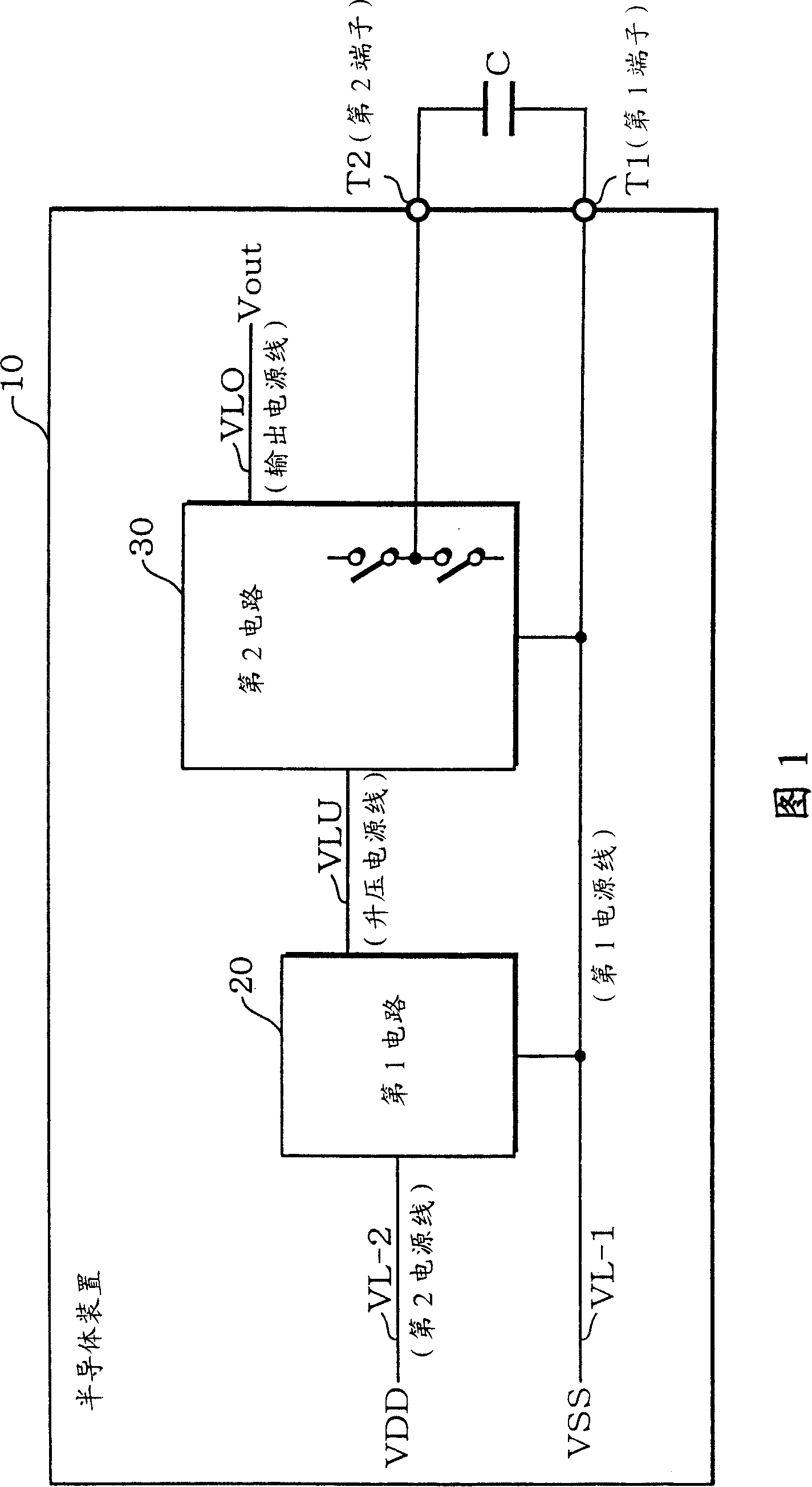
[0081] FIG. 1 is a schematic configuration diagram of a semiconductor device in the first embodiment. The semiconductor device (integrated circuit device (IC), chip) 10 is used to boost the voltage between the first and second power supply lines VL-1 and VL-2 to M×N (M>N, M, N is positive Integer) times to generate the output voltage Vout. The output voltage Vout is output between the first power supply line VL-1 and the output power supply line VLO.

[0082] The semiconductor device 10 includes first and second circuits 20, 30 and first and second terminals T1, T2.

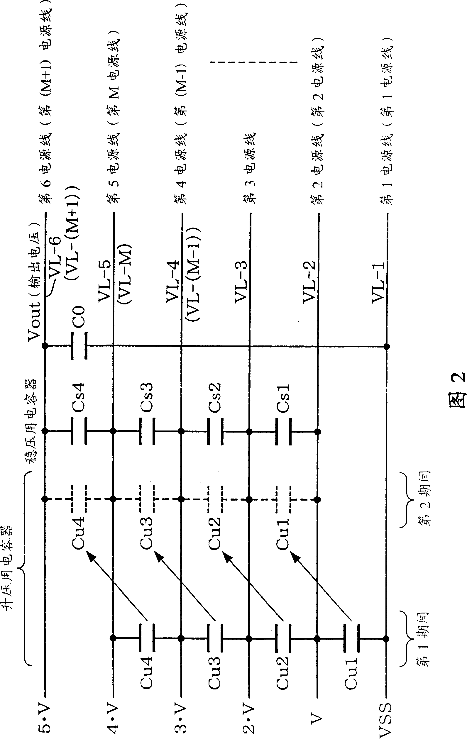
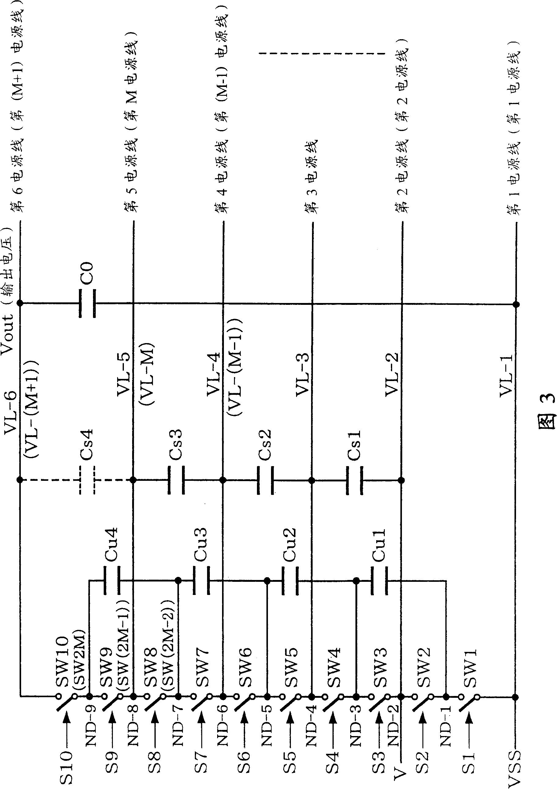
[0083] The first circuit 20 is connected to the first and second power supply lines VL-1, VL-2 and the boosted power supply line VLU. Moreover, the first circuit 20 operates according to the charge pump (Charge Pump), and outputs the voltage M·V obtained by multiplying the voltage VM between the first and second power supply lines VL-1 and VL-2 to the first power supply line. Between VL-1 and the boost power l...


PUM

PropertyMeasurementUnit
thicknessaaaaaaaaaa
thicknessaaaaaaaaaa

Abstract

A first circuit is connected with the first and second power supply lines and a boost power supply line, and outputs a voltage obtained by multiplying the voltage between the first and second power supply lines M times (M is a positive integer), between the first power supply line and the boost power supply line. A second circuit is connected with the first power supply line, the boost power supply line and an output power supply line, and includes a plurality of switching elements. The second circuit outputs a voltage obtained by multiplying the voltage generated in the first circuit N times (M>N, M and N is a positive integer), between the first power supply line and the output power supply line by a charge-pump operation using a capacitor connected between first and second terminals outside and the switching element connected with the second terminal.

Description

technical field [0001] The present invention relates to a semiconductor device and a display device. Background technique [0002] As a display device, a liquid crystal display device having an electro-optical device is generally used. By assembling the liquid crystal display device in electronic equipment, the miniaturization of the electronic equipment and the reduction of current consumption can be achieved simultaneously. [0003] However, driving a liquid crystal display device requires a high voltage. Therefore, it is in line with the viewpoint of cost reduction to incorporate a power supply circuit that generates a high voltage in a driver IC (Integrated Circuit) (semiconductor device in a broad sense) that drives an electro-optical device. At this time, the power supply circuit has a booster circuit. The boost circuit boosts the voltage between the system power supply voltage VDD on the high potential side and the ground power supply voltage VSS on the low potenti...

Claims


Application Information

Patent Timeline
Patent Type & Authority Patents(China)
IPC IPC(8): H02M3/07G09G3/36G02F1/133H01L27/00G09G3/20
CPCG09G3/3696
Inventor 上条治雄
Owner SEIKO EPSON CORP
Why Eureka
Try Eureka