Electro-chemical deposition system and method of electroplating on substrates

a technology of electrochemical deposition and substrate, which is applied in the direction of electric circuits, manufacturing tools, coatings, etc., can solve the problems of aluminum also suffering from electromigration phenomena, many traditional deposition processes have difficulty filling sub-micron structures, and a great amount of ongoing effort being directed at the formation of void-free sub-micron structures, etc., to achieve the effect of easy maintenance of configuration

Inactive Publication Date: 2008-04-08
LANDAU UZIEL
View PDF137 Cites 36 Cited by
  • Summary
  • Abstract
  • Description
  • Claims
  • Application Information

AI Technical Summary

Benefits of technology

[0024]The invention provides an apparatus and a method for achieving reliable, consistent metal electroplating or electrochemical deposition onto substrates. More particularly, the invention provides uniform and void-free deposition of metal onto substrates having sub-micron features formed thereon and a metal seed layer formed thereover. The invention provides an electro-chemical deposition cell comprising a substrate holder, a cathode electrically contacting a substrate plating surface, an electrolyte container having an electrolyte inlet, an electrolyte outlet and an opening adapted to receive a substrate and an anode electrically connect to an electrolyte. The configuration and dimensions of the deposition cell and its components are designed to provide uniform current distribution across the substrate. The cell is equipped with a flow-through anode and a diaphragm unit that provide a combination of relatively uniform flow of particular-free electrolyte in an easy to maintain configuration. Additionally, an agitation device may be mounted to the substrate holder to vibrate the substrate in one or more directions, ie., x, y and / or z directions. Still further, an auxiliary electrode can be disposed adjacent the electrolyte outlet to provide uniform deposition across the substrate surface and to shape as necessary the electrical field at the edge of the substrate and at the contacts. Still further, time variable current waveforms including periodic reverse and pulsed current can be applied during the plating period to provide a void-free metal layer within sub-micron features on the substrate.

Problems solved by technology

Many traditional deposition processes have difficulty filling sub-micron structures where the aspect ratio exceed 2:1, and particularly where it exceeds 4:1.
Therefore, there is a great amount of ongoing effort being directed at the formation of void-free, sub-micron features having high aspect ratios.
However, aluminum has a higher electrical resistivity than other more conductive metals such as copper and silver, and aluminum also can suffer from electromigration phenomena.
Electromigration can lead to the formation of voids in the conductor.
A void may accumulate and / or grow to a size where the immediate cross-section of the conductor is insufficient to support the quantity of current passing through the conductor, and may also lead to an open circuit.
The area of conductor available to conduct heat therealong likewise decreases where the void forms, increasing the risk of conductor failure.
This problem is sometimes overcome by doping aluminum with copper and with tight texture or crystalline structure control of the material.
However, electromigration in aluminum becomes increasingly problematic as the current density increases.
Despite the desirability of using copper for semiconductor device fabrication, choices of fabrication methods for depositing copper into high aspect ratio features are limited.
Precursors for CVD deposition of copper are ill-developed and involve complex and costly chemistry.
Physical vapor deposition into such features produces unsatisfactory results because of limitations in ‘step coverage’ and voids formed in the features.
However, a number of obstacles impair consistent reliable electroplating of copper onto substrates having a sub-micron scale, high aspect ratio features.
Generally, these obstacles involve difficulty with providing uniform current density distribution across the substrate plating surface, which is needed to form a metal layer having uniform thickness.
A primary obstacle is how to get current to the substrate and how to ensure that the current is uniformly distributed thereon.
The ‘excluded’ area can no longer be used to ultimately form devices on the substrate.
However, the contact resistance of the contacts to the seed layer may vary from contact to contact, resulting in a non-uniform distribution of current densities across the substrate.
Also, the contact resistance at the contract to seed layer interface may vary from substrate to substrate, resulting in inconsistent plating distribution between different substrates using the same equipment.
A resistive substrate effect is usually pronounced during the initial phase of the electroplating process and reduces the deposition uniformity because the seed layer and the electroplated layers on the substrate deposition surface are typically thin.
The metal plating tends to concentrate near the current feed contacts, i.e., the plating rate is greatest adjacent the contacts, because the current density across the substrate decreases as the distance from the current feed contacts increases due to insufficient conductive material on the seed layer to provide a uniform current density across the substrate plating surface.
Traditional fountain plater designs also provide non-uniform flow of the electrolyte across the substrate plating surface, which compounds the effects of the non-uniform current distribution on the plating surface by providing non-uniform replenishment of plating ions and where applicable, plating additives, across the substrate, resulting in non-uniform plating.
Such rotation introduces complexity into the plating cell design due to the need to furnish current across and revolving interface.
However, the plating uniformity still deteriorates at the boundaries or edges of the substrate because of the fringing effects of the electrical field near the edge of the substrate, the seed layer resistance and the potentially variable contact resistance.
There is also a problem in maintaining an electroplating solution to the system having consistent properties over the duration of a plating cycle and / or over a run of multiple wafers being plated.
The metal electrolyte replenishing scheme is difficult to control and causes build-up of co-ions in the electrolyte, resulting in difficult to control variations in the ions concentration in the electrolyte.
Thus, the electroplating process produces inconsistent results because of inconsistent ion concentration in the electrolyte.
Additionally, operation of a plating cell incorporating a non-consumable anode may cause bubble-related problems because oxygen evolves on the anode during the electroplating process.
Bubble-related problems include plating defects caused by bubbles that reach the substrate plating surface and prevent adequate electrolyte contact with the plating surface.

Method used


Image

  • Electro-chemical deposition system and method of electroplating on substrates
  • Electro-chemical deposition system and method of electroplating on substrates
  • Electro-chemical deposition system and method of electroplating on substrates

Examples


Embodiment Construction

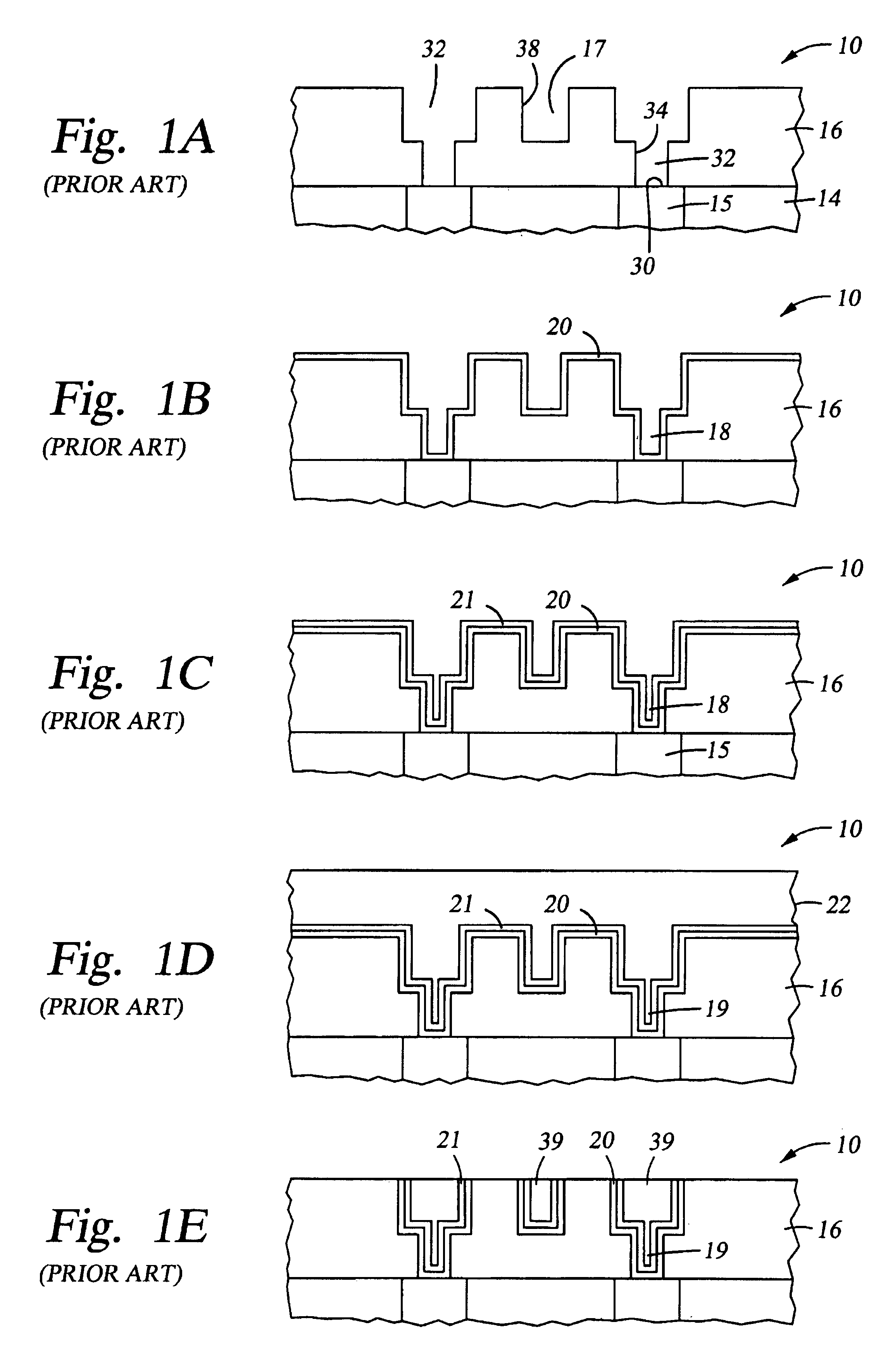
[0035]The present invention generally provides several embodiments of a new electrochemical cell and a method of operation of the cells to deposit high quality metal layers on substrates. The invention also provides new electrolyte solutions which can be used to advantage in the deposition of metals, and copper in particular, into very small features, i.e., micron sized features and smaller. The invention will be described below first in reference to the hardware, then operation of the hardware and then chemistry of the electrolyte solutions.

[0036]Electrochemical Cell Hardware

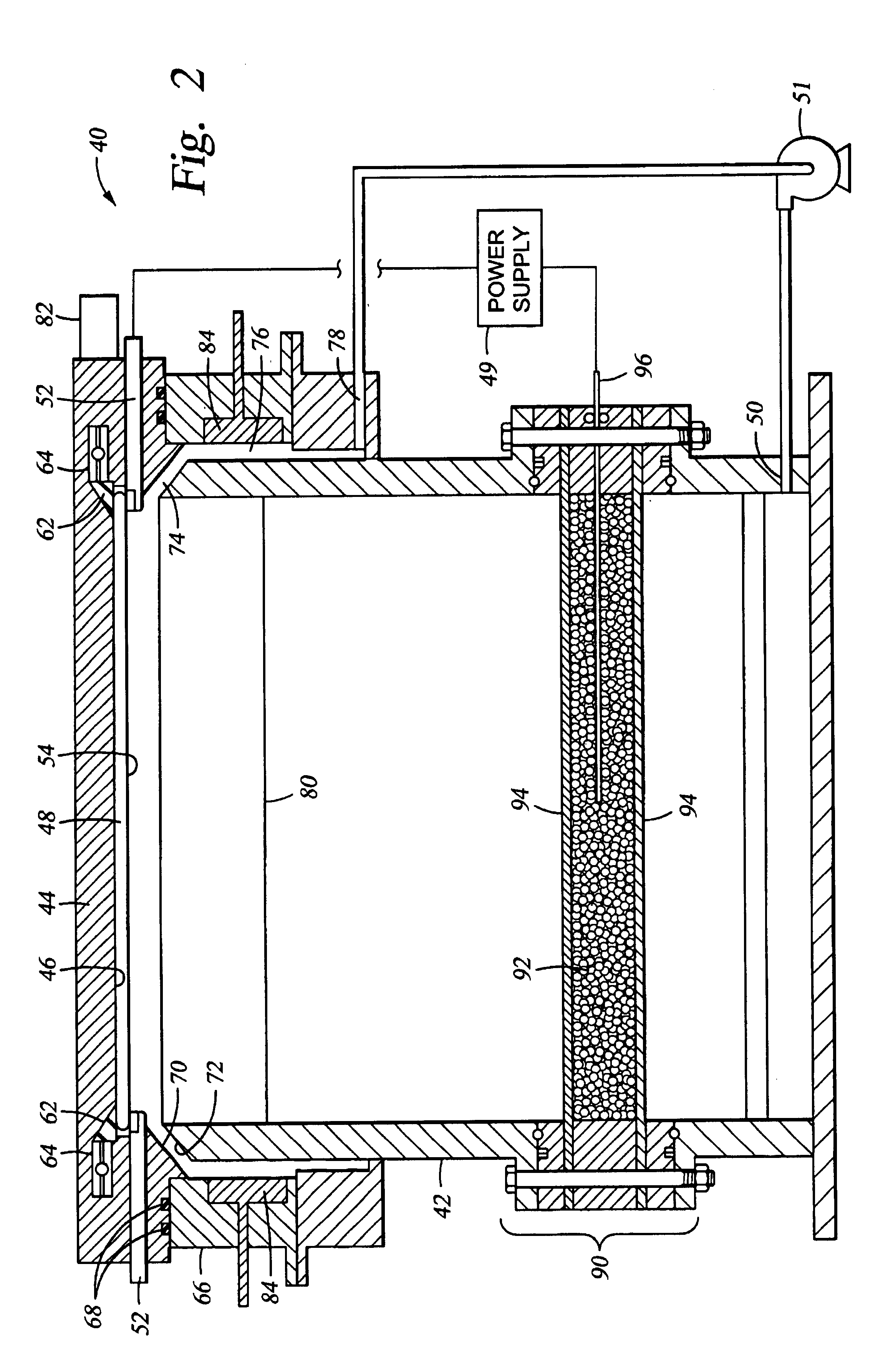
[0037]FIG. 2 is a cross sectional schematic view of a cell 40 for electroplating a metal onto a substrate. The electroplating cell 40 generally comprises a container body 42 having an opening on the top portion of the container body to receive and support a substrate holder 44 thereover. The container body 42 is preferably an annular cell comprised of an electrically insulative material, such a plastic, plexigl...


PUM

PropertyMeasurementUnit
gap widthaaaaaaaaaa
gap widthaaaaaaaaaa
cathodic current densityaaaaaaaaaa

Abstract

The invention provides an apparatus and a method for achieving reliable, consistent metal electroplating or electrochemical deposition onto semiconductor substrates. More particularly, the invention provides uniform and void-free deposition of metal onto metal seeded semiconductor substrates having sub-micron, high aspect ratio features. The invention provides an electrochemical deposition cell comprising a substrate holder, a cathode electrically contacting a substrate plating surface, an electrolyte container having an electrolyte inlet, an electrolyte outlet and an opening adapted to receive a substrate plating surface and an anode electrically connect to an electrolyte. Preferably, a vibrator is attached to the substrate holder to vibrate the substrate in at least one direction, and an auxiliary electrode is disposed adjacent the electrolyte outlet to provide uniform deposition across the substrate surface. Preferably, a periodic reverse current is applied during the plating period to provide a void-free metal layer within high aspect ratio features on the substrate.

Description

CROSS REFERENCE TO RELATED APPLICATION[0001]This application claims the benefit of U.S. Provisional Application Ser. No. 60 / 082,521, entitled “Electroplating on Substrates,” filed on Apr. 21, 1998.BACKGROUND OF THE INVENTION[0002]1. Field of the Invention[0003]The present invention generally relates to deposition of a metal layer onto a substrate. More particularly, the present invention relates to an apparatus and a method for electroplating a metal layer onto a substrate.[0004]2. Background of the Related Art[0005]Sub-micron multi-level metallization is one of the key technologies for the next generation of ultra large scale integration (ULSI). The multilevel interconnects that lie at the heart of this technology require planarization of interconnect features formed in high aspect ratio apertures, including contacts, vias, lines and other features. Reliable formation of these interconnect features is very important to the success of ULSI and to the continued effort to increase cir...

Claims


Application Information

Patent Timeline
Patent Type & Authority Patents(United States)
IPC IPC(8): C25D5/00C25D17/00C25D3/38C25D7/12
CPCC25D3/38C25D17/001C25D7/123C25D17/00
Inventor LANDAU, UZIEL
Owner LANDAU UZIEL
Why Eureka
Try Eureka