Card and card production method
a production method and card technology, applied in the field of cards, can solve problems such as deterioration in production efficiency, insufficient heating and pressing, and problems in external appearance, and achieve the effect of improving external appearan
- Summary
- Abstract
- Description
- Claims
- Application Information
AI Technical Summary
Benefits of technology
Problems solved by technology
Method used
Image

Examples
first embodiment
[0050]A first embodiment of the present invention will be described below referring to the drawings
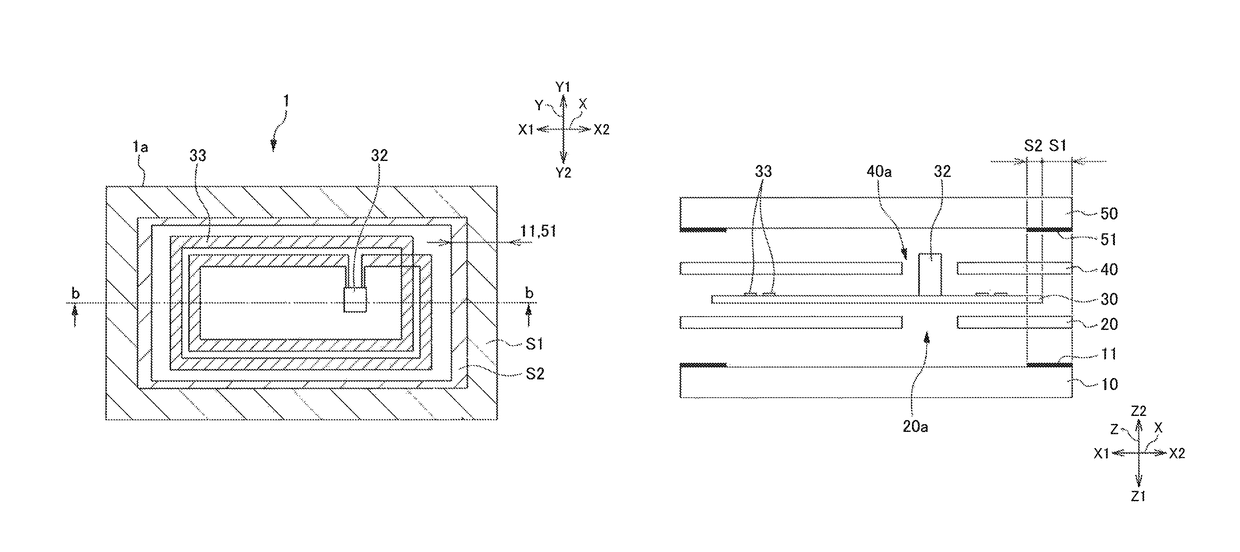
[0051]FIGS. 1A and 1B illustrate a plan view and a cross-sectional view of the card 1 according to the first embodiment.
[0052]FIG. 1A is a plan view of the card 1.
[0053]FIG. 1B is a cross-sectional view (cross-sectional view taken along the section b-b in FIG. 1A) depicting the laminate-structure of the card 1 before each layer is bonded.
[0054]In the embodiment and the drawing, the direction normal to the card surface is defined as the up-and-down direction Z, and the figure viewed from the direction Z is defined as the plan view. In the plan view of the card 1, the direction along the longer side is defined as the right-and-left direction X and the direction along the shorter side is defined as the longitudinal direction Y. The shape in the plan view is referred to as a plane shape as required.
[0055]Note that to clearly illustrate the configuration in each drawing, dimensions may be m...
second embodiment
[0147]Now, a second embodiment of the present invention will be described.
[0148]In the description and the drawing of the embodiment below, the portion having the same function as the first embodiment described above is appended with the same reference sign or a reference sign including the same reference sign in the right hand digit or digits, and any repeated explanation is suitably omitted.
[0149]FIG. 8 depicts the laminate-structure of a card 201 according to the second embodiment.
[0150]FIGS. 9A to 9C depict a production step of the card 201 according to the second embodiment.
[0151]FIG. 9A corresponds to FIG. 4C.
[0152]FIG. 9B corresponds to FIG. 4D.
[0153]FIG. 9C corresponds to FIG. 5F.
[0154]As illustrated in FIG. 8, the card 201 does not include the upper spacer sheet since the IC chip 232 is thinner than the first embodiment.
[0155]As illustrated in FIG. 9A, in the high pressure maintaining step, the laminated body 202 is sandwiched between the heat pressing plates 81 and 82.
[015...
third embodiment
[0159]Now a third embodiment of the present invention will be described.
[0160]FIGS. 10A to 10C depict the laminate-structure and the production step of the card 301 according to the third embodiment.
[0161]As illustrated in FIG. 10A, only a wiring pattern 333 and a thin electronic component (not shown in the drawing) are mounted on a module substrate 330, but a thick electronic component such as an IC chip is not mounted. Therefore, the card 301 does not require the upper spacer sheet or the lower spacer sheet so that a lower layer 310 and an upper layer 350 are directly laminated on the module substrate 330.
[0162]Even in this case, the card 301 can increase the contact pressure between the lower layer 310 and the upper layer 350 in a substrate outer region S301 by the effect of thickness adjustment layers 311 and 351.
[0163]In this manner, similarly to the first embodiment, the card 301 can improve production efficiency.
PUM
| Property | Measurement | Unit |
|---|---|---|
| thickness | aaaaa | aaaaa |
| temperature | aaaaa | aaaaa |
| pressure P1 | aaaaa | aaaaa |
Abstract
Description
Claims
Application Information
 - R&D
- Intellectual Property
- Life Sciences
- Materials
- Tech Scout
- Unparalleled Data Quality
- Higher Quality Content
- 60% Fewer Hallucinations
Browse by: Latest US Patents, China's latest patents, Technical Efficacy Thesaurus, Application Domain, Technology Topic, Popular Technical Reports.
© 2025 PatSnap. All rights reserved.Legal|Privacy policy|Modern Slavery Act Transparency Statement|Sitemap|About US| Contact US: help@patsnap.com