Biscarbazole derivative host materials for OLED emissive region

a technology of emissive region and host material, which is applied in the field of organic electroluminescent devices, can solve the problems of cbp being easily deteriorated by, not suitable for practical use, and known to have a very short life, and achieves the effects of improving life time, low voltage requirement, and high luminous efficiency

Active Publication Date: 2018-05-29
IDEMITSU KOSAN CO LTD +1
View PDF19 Cites 0 Cited by
  • Summary
  • Abstract
  • Description
  • Claims
  • Application Information

AI Technical Summary

Benefits of technology

[0070]The inventors have found that the organic EL devices containing the host materials and phosphorescent materials according to the present disclosure exhibit low voltage requirement with high luminous efficiency. Additionally, the devices having the co-host combinations in the emitting layer according to the present disclosure exhibited an additional benefit of improved life time of more than 3 times when compared to a single-host example device.
[0071]A luminous efficiency and a lifetime of the multilayered organic EL device depend on a carrier balance of the entire organic EL device. The main factors that control the carrier balance are carrier transporting capability of each of the organic layers and carrier injecting capability in the interfacial region of separate organic layers. In the organic EL devices having the co-host combinations of the present disclosure, the co-host materials provide an improved charge carrier balance of the entire organic EL device by putting two of positive hole transportability materials and electronic transportability materials together. The provision of such co-host materials reduces deterioration by the carrier invasion to the adjacent layer.
[0072]For example, the inventors have found that the emitter host materials represented by the formulas (1A) and (2A) in the present disclosure not only function well as a single host in an emitter layer but also as cohosts. This is because the organic compounds represented by the formulas (1A) and (2A) have a biscarbazole skeleton having an excellent hole transporting capability as well as a heterocyclic skeleton having an excellent electron transporting capability. Providing these two compounds as cohosts in the emitter layer, the carrier injecting capability to neighboring layers in the emitting layer (recombination region) is balanced.

Problems solved by technology

However, CBP is known to have a very short lifetime, and therefore it is not suitable for practical use in EL devices such as an OLED.
Without being bound by scientific theory, it is believed that this is because CBP may be heavily deteriorated by a hole due to its oxidative stability not being high, in terms of molecular structure.
The current efficiency and the lifetime are improved by the above technique, but it is not satisfactory in a certain case for practical use.
Thus, energy transfer to a phosphorescent dopant having an emission wavelength in a visible light region of 500 nm to 720 nm cannot be achieved using such a host, since the excited state triplet energy would be quenched by a host having such a low triplet state energy.
Accordingly, anthracene derivatives are unsuitable as a phosphorescent host.
Such an arrangement has the drawback of a likelihood of crystallization of the light emitting layer.
However, the efficiency of these materials as a phosphorescent host is not disclosed.
However, the effectiveness of these materials as a phosphorescent host is not disclosed.
However, the effectiveness of an OLED prepared by combining such materials with a phosphorescent material is not disclosed, and the application discloses perylene and pyrene rings which are known to have a small triplet energy level as condensed polycyclic aromatic rings, and which are not preferred for use as a light emitting layer of a phosphorescent device, and materials which are effective for a phosphorescent device are not selected.

Method used


Image

  • Biscarbazole derivative host materials for OLED emissive region
  • Biscarbazole derivative host materials for OLED emissive region
  • Biscarbazole derivative host materials for OLED emissive region

Examples


Embodiment Construction

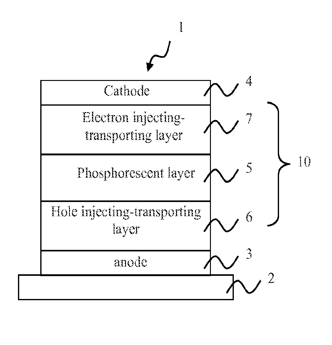
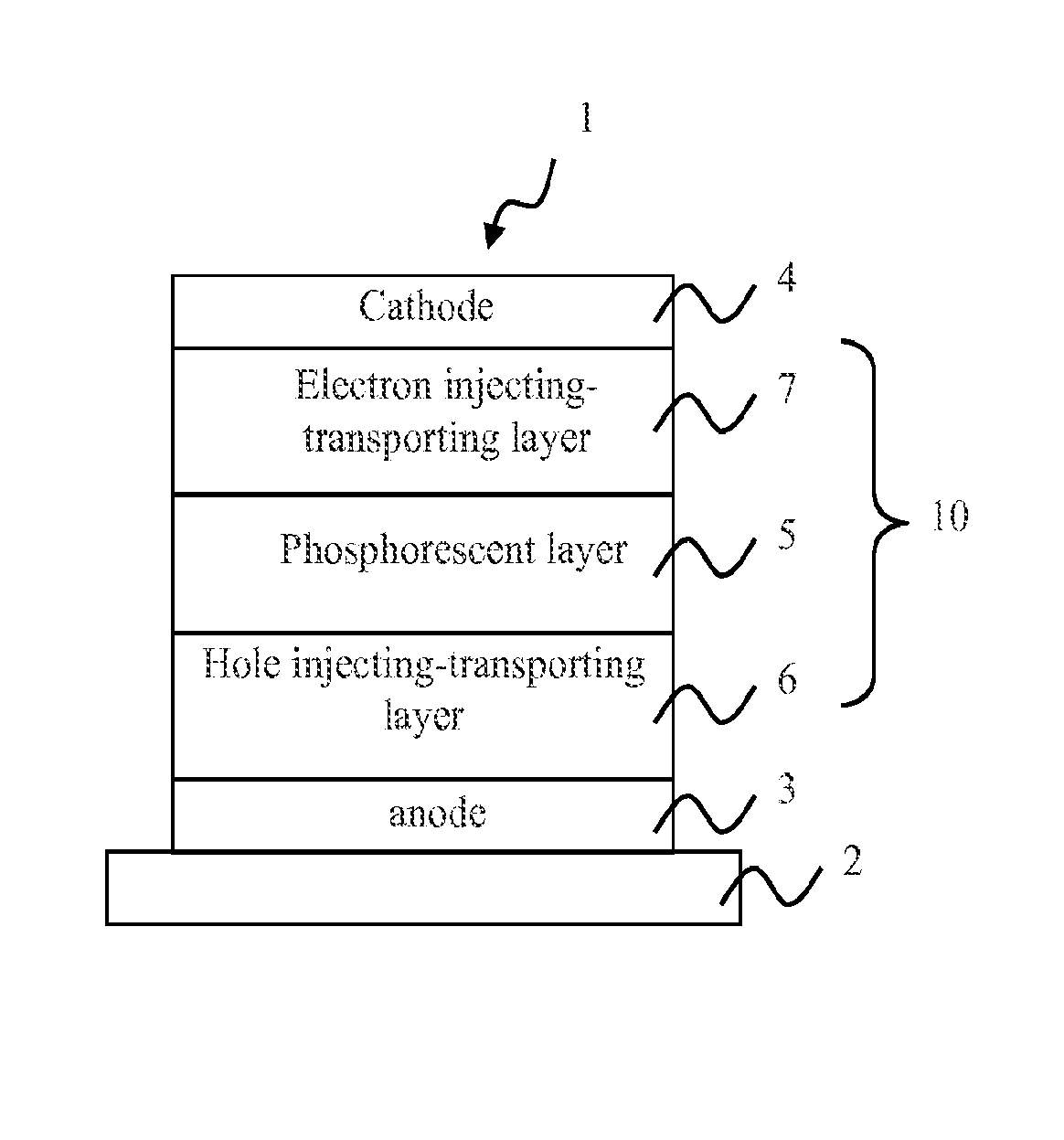
[0074]The OLEDs of the present invention may comprise a plurality of layers located between an anode and a cathode. Representative OLEDs according to the invention include, but are not limited to, structures having constituent layers as described below:[0075](1) anode / light emitting layer / cathode;[0076](2) anode / hole injecting layer / light emitting layer / cathode;[0077](3) anode / light emitting layer / electron injecting⋅transporting layer / cathode;[0078](4) anode / hole injecting layer / light emitting layer / electron injecting⋅transporting layer / cathode;[0079](5) anode / organic semiconductor layer / light emitting layer / cathode;[0080](6) anode / organic semiconductor layer / electron blocking layer / light emitting layer / cathode;[0081](7) anode / organic semiconductor layer / light emitting layer / adhesion improving layer / cathode;[0082](8) anode / hole injecting⋅transporting layer / light emitting layer / electron injecting⋅transporting layer / cathode;[0083](9) anode / insulating layer / light emitting layer / insulat...


PUM

PropertyMeasurementUnit
quantum efficiencyaaaaaaaaaa
internal quantum efficienciesaaaaaaaaaa

Abstract

An organic electroluminescence device utilizes a novel combination of one or more biscarbazole derivative compounds as the phosphorescent host material in combination with an organometallic phosphorescent material as a dopant in the light emitting region of the device, where the biscarbazole derivative compounds are represented by a formula (1A) or (2A) below: where A1 represents a substituted or unsubstituted nitrogen-containing heterocyclic group having 1 to 30 ring carbon atoms; A2 represents a substituted or unsubstituted aromatic hydrocarbon group having 6 to 30 ring carbon atoms, or substituted or unsubstituted nitrogen-containing heterocyclic group having 1 to 30 ring carbon atoms; X1 and X2 each are a linking group; Y1 to Y4 each represent a substituent; p and q represent an integer of 1 to 4; and r and s represent an integer of 1 to 3; and the organometallic phosphorescent material is a compound having a substituted chemical structure represented by the formula (4A): where each R is independently selected from the group consisting of H, alkyl, alkenyl, alkynyl, alkylaryl, CN, CF3, CnF2n+1, trifluorovinyl, CO2R, C(O)R, NR2, NO2, OR, halo, aryl, heteroaryl, substituted aryl, substituted heteroaryl or a heterocyclic group; M is a platinum group metal; Ar′, Ar″, Ar′″ and Ar″″ each independently represent a substituted or unsubstituted aryl or heteroaryl substituent on the phenylpyridine ligand; a is 0 or 1; b is 0 or 1; c is 0 or 1; d is 0 or 1; m is 1 or 2; n is 1 or 2; m+n is the maximum number of ligands that can be coordinated to M, and wherein at least one of a, b, c, and d is 1 and when at least one of a and b is 1 and at least one of b and c is 1, at least one of Ar′ and Ar″ is different from at least one of Ar′″ and Ar″″.

Description

BACKGROUND OF THE INVENTION[0001]The present invention relates to an organic electroluminescent (EL) device such as an organic light emitting device (hereinafter abbreviated as an OLED) and materials capable of being used in such an OLED. In particular, it relates to an OLED which comprises a light emitting layer which emits a green light, and materials for an OLED which are used for the same.RELATED ART[0002]OLEDs which comprise an organic thin film layer which includes a light emitting layer located between an anode and a cathode are known in the art. In such devices, emission of light may be obtained from exciton energy, produced by recombination of a hole injected into a light emitting layer with an electron.[0003]Generally, OLEDs are comprised of several organic layers in which at least one of the layers can be made to electroluminesce by applying a voltage across the device. When a voltage is applied across a device, the cathode effectively reduces the adjacent organic layers ...

Claims


Application Information

Patent Timeline
Patent Type & Authority Patents(United States)
IPC IPC(8): H01L51/00H01L51/50C07D209/82C09K11/06C07D401/14C07D405/14H05B33/20
CPCH01L51/5016C07D209/82C07D401/14C07D405/14C09K11/06H01L51/0072H05B33/20C09K2211/1007C09K2211/1029C09K2211/185H01L51/0059H01L51/0067H01L51/0073H01L51/0085H01L51/5012H01L2251/5384H10K85/631H10K85/654H10K85/6572H10K85/342H10K50/11H10K2101/90H10K85/6574H10K2101/10
Inventor NISHIMURA, KAZUKIIWAKUMA, TOSHIHIROYAMAMOTO, HITOSHIWEAVER, MICHAEL S.BROWN, JULIA J.
Owner IDEMITSU KOSAN CO LTD
Why Eureka
Try Eureka