
Organic light-emitting diode display

a light-emitting diode and display technology, applied in the direction of semiconductor devices, electrical apparatus, transistors, etc., can solve the problems of change in luminance, affecting the voltage of the data line, process design does not allow continuous reduction, etc., to minimize the parasitic capacitance, minimize the vertical crosstalk, and minimize the kickback voltage

Active Publication Date: 2018-02-20
SAMSUNG DISPLAY CO LTD
View PDF23 Cites 1 Cited by
  • Summary
  • Abstract
  • Description
  • Claims
  • Application Information

AI Technical Summary

Benefits of technology

The patent text describes an OLED display that can minimize vertical crosstalk, which is the interference between neighboring pixels. The invention does this by positioning a semiconductor layer or a portion of the light emission control line between the scan line and the data line, which reduces parasitic capacitance and kicker back voltage. This allows for a larger driving range and more precise control of light intensity, resulting in higher display resolution and improved quality.

Problems solved by technology

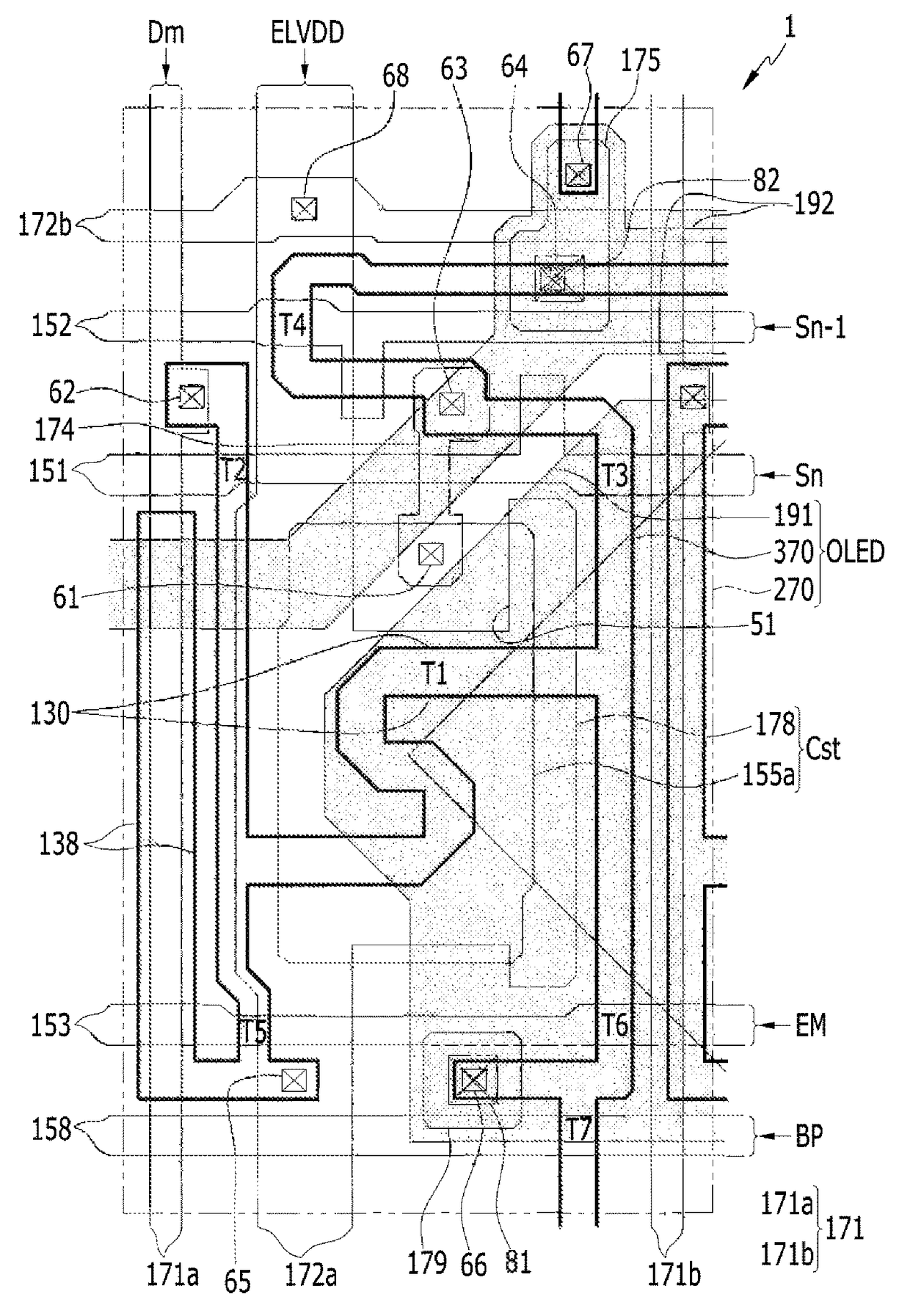
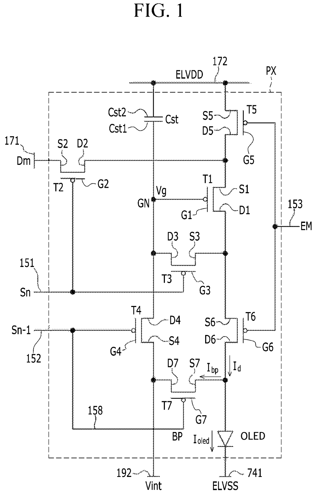
However, a change in voltage of the data line affects a voltage of a driving gate node of the driving transistor due to a parasitic capacitance formed between a driving gate node and a data line connected to a driving gate electrode of the driving transistor.
The change in voltage of the driving gate node changes a driving current flowing in the OLED to cause vertical crosstalk which leads to a change in luminance.
Process design does not allow for continuous reduction due to a limitation of facility specification and photolithography process capability, such that there is a limitation in minimizing the vertical crosstalk.

Method used


Image

  • Organic light-emitting diode display
  • Organic light-emitting diode display
  • Organic light-emitting diode display

Examples


Embodiment Construction

[0054]The described technology will be described more fully hereinafter with reference to the accompanying drawings, in which exemplary embodiments are shown.

[0055]As those skilled in the art would realize, the described embodiments can be modified in various different ways, all without departing from the spirit or scope of the described technology.

[0056]Accordingly, the drawings and description are to be regarded as illustrative in nature and not restrictive. Like reference numerals designate like elements throughout the specification.

[0057]In addition, the size and thickness of each configuration shown in the drawings are arbitrarily shown for understanding and ease of description, but the described technology is not limited thereto. In the drawings, the thickness of layers, films, panels, regions, etc., are exaggerated for clarity. In the drawings, for understanding and ease of description, the thickness of some layers and areas is exaggerated.

[0058]In addition, unless explicitly...


PUM


Abstract

An organic light-emitting diode display is disclosed. The display includes a semiconductor layer formed over a substrate, a scan line formed over the semiconductor layer and configured to provide a scan signal, and a light emission control line formed over the semiconductor layer and configured to provide a light emission control signal. The display includes a data line configured to provide a data voltage and a driving voltage line configured to provide a driving voltage, wherein the driving voltage line crosses the scan line and is electrically insulated from the scan line. A switching transistor is electrically connected to the scan line and the data line and includes a switching drain electrode. A driving transistor includes a driving source electrode electrically connected to the switching drain electrode. Any one of the semiconductor layer and the light emission control line includes an extension at least partially overlapping the data line.

Description

CROSS-REFERENCE TO RELATED APPLICATION[0001]This application is a continuation of U.S. patent application Ser. No. 14 / 939,819, filed Nov. 12, 2015 U.S. Pat. No. 9,761,646, which claims priority to and the benefit of Korean Patent Application No. 10-2015-0060609, filed on Apr. 29, 2015, the entire contents of both of which are incorporated herein by reference.[0002]U.S. patent application Ser. No. 14 / 939,819 relates to U.S. patent application Ser. No. 14 / 939,837, also filed Nov. 12, 2015, the entire content of which is incorporated herein by reference.BACKGROUND1. Field of the Invention[0003]The described technology generally relates to an organic light-emitting diode display.2. Description of the Related Art[0004]An organic light-emitting diode (OLED) includes two electrodes and an interposed organic emission layer. The OLED forms excitons by combining electrons injected from a cathode electrode with holes injected from an anode electrode at the organic emission layer and emits ligh...

Claims


Application Information

Patent Timeline
Patent Type & Authority Patents(United States)
IPC IPC(8): H01L27/32H01L29/786
CPCH01L27/3262H01L29/78696H01L27/3276H01L27/3265H01L27/1255H10K59/1216H10K59/1213H10K59/131
Inventor LEEHYUN, CHAE HANEOM, KI MYEONG
Owner SAMSUNG DISPLAY CO LTD
Learn More