Optical module and method of manufacturing the same

a technology of optical modules and optical fibers, applied in the field of optical modules, can solve the problems of optical distortion phenomenon, optical signal loss, and very often insufficient cutting of optical fibers, and achieve the effect of maximizing optical efficiency and maximizing optical efficiency

Active Publication Date: 2017-09-19
YOTTAHN INC
View PDF15 Cites 37 Cited by
  • Summary
  • Abstract
  • Description
  • Claims
  • Application Information

AI Technical Summary

Benefits of technology

[0024]The cover block may further include a step jaw that protrudes from the bottom surface of the second body of the cover between the lens assembly and the injection port. The step jaw may limit movements of the ends of the one or more optical fibers.
[0025]According to another aspect of the present disclosure, a method of manufacturing an optical module includes printing wiring on a top surface of a substrate. One or more reference marks are printed on the top surface of the substrate. One or more optical devices and an integrated circuit (IC) device are mounted on the wiring. An optical bench are aligned and attached onto the substrate by referring to the one or more reference marks. A cover is attached to the optical bench. One or more optical fibers are inserted into a space between the optical bench and the cover. Vertical and horizontal directions of the one or more optical fibers are adjusted while holding the one or more optical fibers from outside the optical bench to find positions for the one or more optical fibers that maximizes an optical efficiency thereof. The one or more optical fibers are fixed to the position that maximizes there optical efficiency.

Problems solved by technology

Meanwhile, due to its cutting characteristic, an optical fiber is very often not cut properly, and its cut surface may be slightly tilted or inclined, which causes an optical distortion phenomenon or an optical signal loss.

Method used


Image

  • Optical module and method of manufacturing the same
  • Optical module and method of manufacturing the same
  • Optical module and method of manufacturing the same

Examples


Embodiment Construction

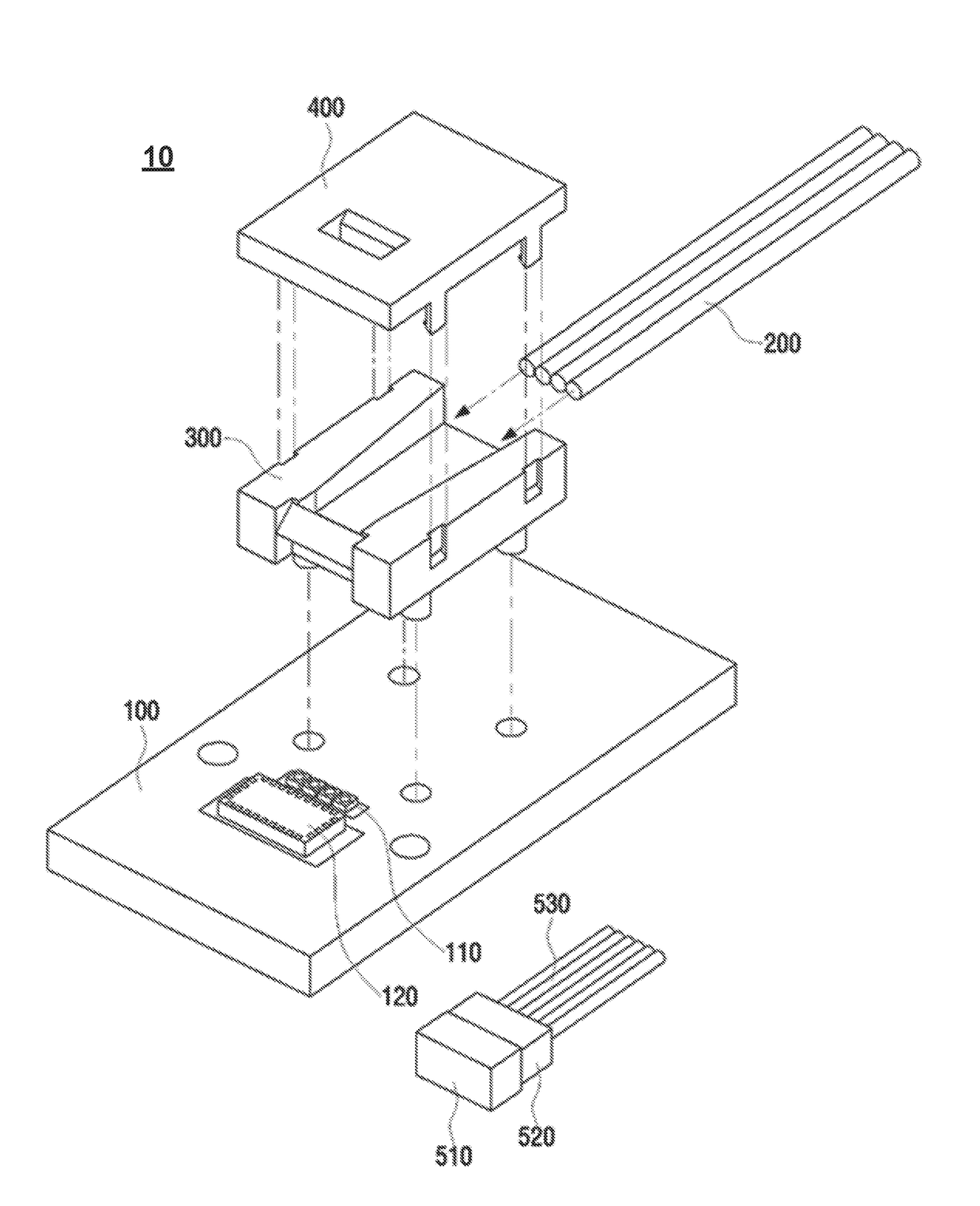
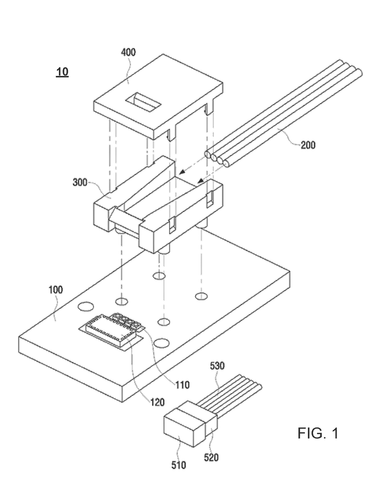
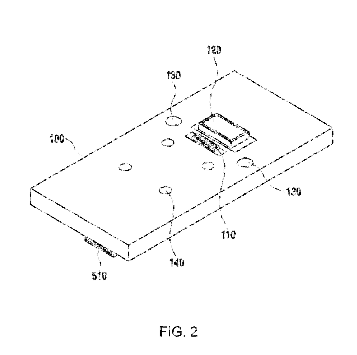
[0040]The disclosure and the various features and advantageous details thereof are explained more fully with reference to the non-limiting embodiments and examples that are described and / or illustrated in the accompanying drawings and detailed in the following description. It should be noted that the features illustrated in the drawings are not necessarily drawn to scale, and features of one embodiment may be employed with other embodiments as the skilled artisan would recognize, even if not explicitly stated herein. Descriptions of well-known components and processing techniques may be omitted so as to not unnecessarily obscure the embodiments of the disclosure. The examples used herein are intended merely to facilitate an understanding of ways in which the disclosure may be practiced and to further enable those of skill in the art to practice the embodiments of the disclosure. Accordingly, the examples and embodiments herein should not be construed as limiting the scope of the dis...


PUM


Abstract

There is provided an optical module, which includes a substrate; one or more optical devices disposed on the substrate; an integrated circuit (IC) device disposed on the substrate for driving the one or more optical devices; one or more optical fibers in optical communications with the one or more optical devices, respectively; an optical bench that attaches to the substrate and concentrates a direction of the light transmitted between the one or more optical devices and the one or more optical fibers; and a cover that attaches to the optical bench with the one or more optical fibers fixed therebetween. The optical bench changes a direction of the concentrated light.

Description

BACKGROUND[0001]1. Field of the Disclosure[0002]The present disclosure relates to an optical module and a method of manufacturing the same.[0003]2. Background of the Disclosure[0004]As various multimedia services have emerged recently, the necessity for exchanging a large amount of information has increased and the amount of data to be transmitted via networks has also increased. Since the introduction of high definition (HD) and ultra high definition (UHD) media broadcasting and streaming services, the conventional copper wire-based data transmission has reached its capacity limit, and optical fiber-based data transmission has become a new mainstream. The data transmission via the optical fibers is not susceptible to electromagnetic interference. With the broadband data transmission capability, optical fibers are widely used for large-capacity transmission of digital media including, for example, HD and UHD digital video broadcasting and streaming services.[0005]An optical module o...

Claims


Application Information

Patent Timeline
Patent Type & Authority Patents(United States)
IPC IPC(8): G02B6/42G02B6/32G02B6/34
CPCG02B6/4244G02B6/4206G02B6/4239G02B6/4214G02B6/4243G02B6/4224G02B6/32G02B6/34
Inventor KIM, HYOGYEOM
Owner YOTTAHN INC
Why Eureka
Try Eureka