
Chemical for forming protective film

a protective film and chemical technology, applied in the field of cleaning, can solve the problems of increasing the aspect ratio, serious damage to the wafer due to its basicity, and solving the problem of damage to the wafer due to cleaning, and achieve the effect of excellent water repellency

Active Publication Date: 2017-06-27
CENT GLASS CO LTD
View PDF17 Cites 3 Cited by
  • Summary
  • Abstract
  • Description
  • Claims
  • Application Information

AI Technical Summary

Benefits of technology

[0043]A protective film formed by a liquid chemical for forming a protective film, according to the present invention is excellent in water repellency, and therefore reduces the capillary force of an unevenly patterned surface of a wafer, and by extension brings about a pattern collapse-preventing effect. With the use of the liquid chemical, a cleaning step conducted in a process for producing the wafer formed having a finely unevenly patterned surface is improved without lowering throughput. Accordingly, the process for producing the wafer formed having the finely unevenly patterned surface, the process being conducted by using the liquid chemical for forming a protective film of the present invention, is excellent in productivity.
[0044]The liquid chemical for forming a protective film, according to the present invention is adaptable to uneven patterns having aspect ratios expected to rise more and more, for example, to an aspect ratio of not less than 7, and therefore allows cost reduction in producing more sophisticated semiconductor devices. In addition to this, the liquid chemical is adaptable without considerably modifying conventional apparatuses, so as to be able to become one applicable in production of various kinds of semiconductor devices.BRIEF EXPLANATION OF THE DRAWINGS
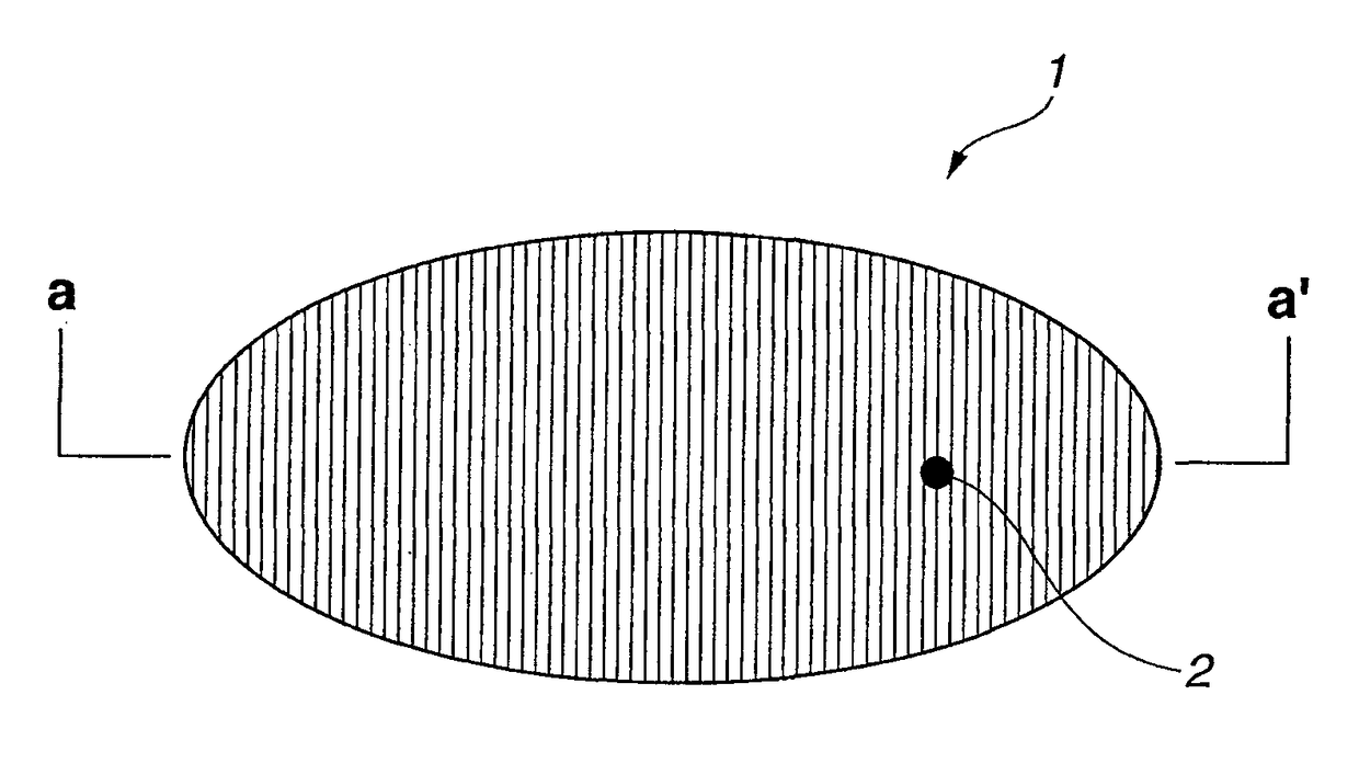
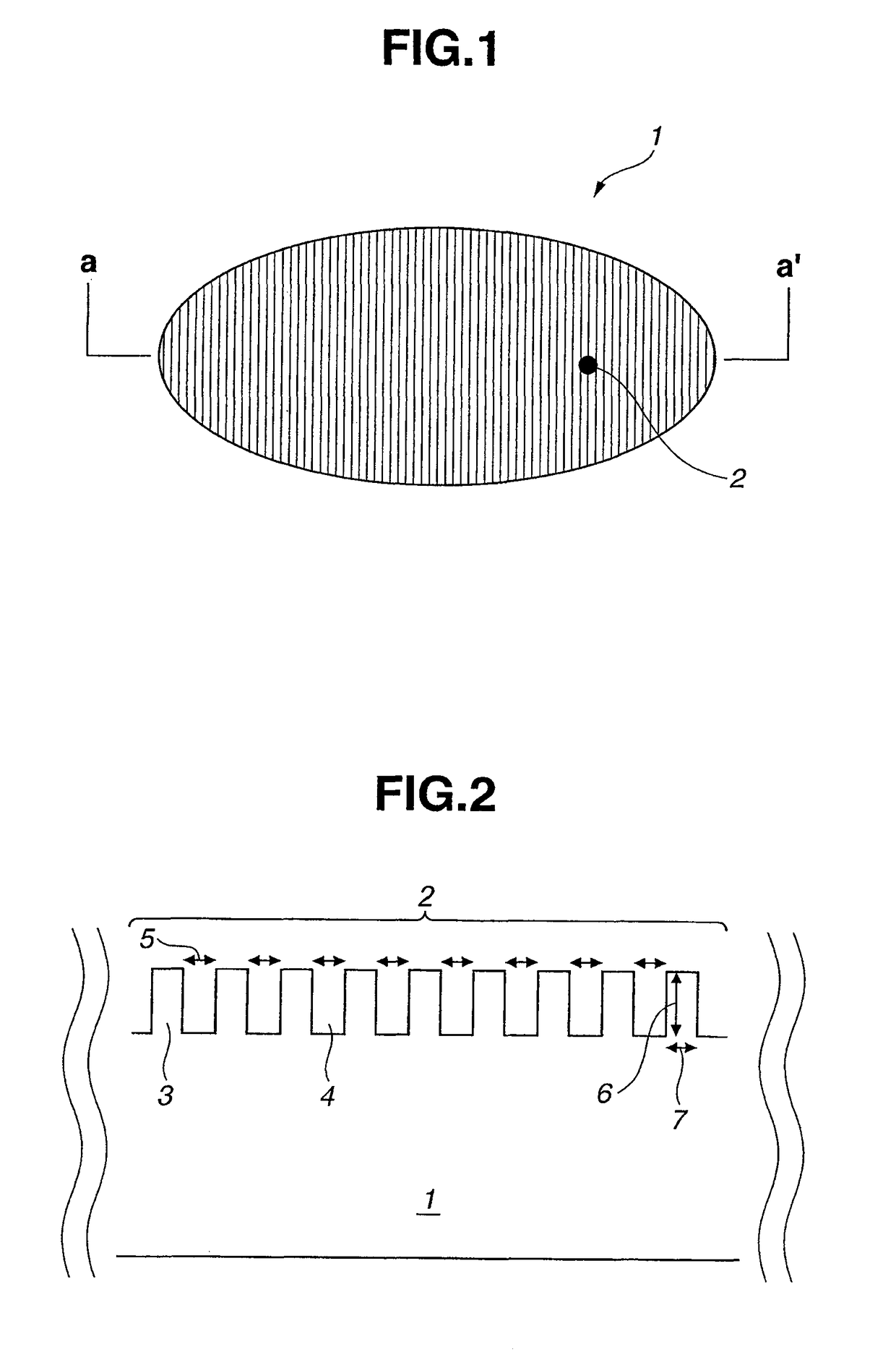
[0045]FIG. 1 A schematic plan view of a wafer 1 whose surface is made into a surface having a finely uneven pattern 2.
[0046]FIG. 2 A view showing a part of a-a′ cross section of FIG. 1.
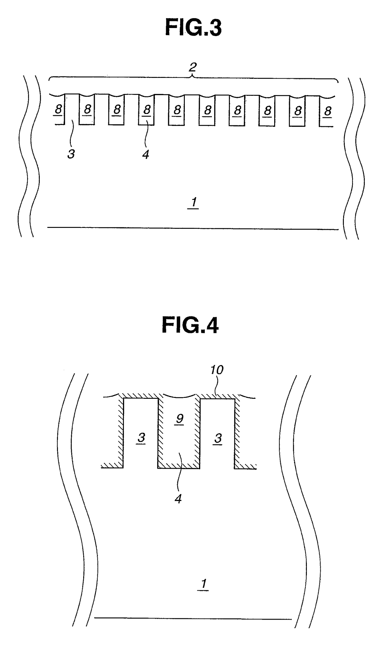
[0047]FIG. 3 A schematic view showing a liquid chemical 8 for forming a protective film is retained in recessed portions 4 in a cleaning step.
[0048]FIG. 4 A schematic view showing a condition where a water-based cleaning liquid is retained in the recessed portions 4 on which the protective film is formed.DETAILED DESCRIPTION

Problems solved by technology

On the other hand, in cleaning conventionally performed by using a mixed ammonia cleaning agent, damages to the wafer due to its basicity are getting serious with the trend toward micro-patterning for circuits.
With this, problems about the damages to the wafer due to cleaning have been solved; however, problems due to an aspect ratio increased with the trend toward micro-processing in the semiconductor devices have become obvious.
In other words, a phenomenon where the pattern is collapsed when a gas-liquid interface passes through the pattern is brought about after cleaning or rinsing so as to largely reduce the yield, which has become a significant problem.
This method is effective for preventing the pattern collapse; however, a solvent having small γ such as 2-propanol and the like is also small in normal contact angle, which results in the trend to increase cos θ. It is therefore said that there are limitations to adaptable patterns, for example, an aspect ratio of not higher than 5.
However, the disclosed technique cannot be applied to the present object because: the technique is one directed to the resist pattern or one for reforming a resist itself; and a final removal together with the resist is possible so as not to need the assumption about a method of removing a treatment agent after drying.
However, any of these is difficult to apply to a mass-producing process because of its poorer throughput than in conventional cleaning steps, though effective to some extent.

Method used


Image

  • Chemical for forming protective film
  • Chemical for forming protective film
  • Chemical for forming protective film

Examples


example 1

(1) Preparation of Liquid Chemical for Forming Protective Film

[0164]A mixture of: 3 g of semiconductor-grade trimethylmethoxysilane [(CH3)3SiOCH3] that serves as a silicon compound (A); 1 g of semiconductor-grade trifluoromethanesulfonic acid [CF3SO3H] that serves as an acid; and 96 g of a semiconductor-grade fluorine-based solvent (Novec HFE-7100 produced by 3M Limited: Hydrofluoroether) that serves as an organic solvent was prepared to obtain a liquid chemical for forming a protective film. Furthermore, a water content was removed from the liquid chemical by using a molecular sieve 4 A (produced by UNION SHOWA K.K.). Thereafter, metal impurities were removed from the liquid chemical by using an ion-exchange resin (IonKleen™ SL Purifier produced by Pall Corporation), followed by removing particles from the liquid chemical by filtration separation (Optimizer produced by Nihon Entegris K.K.), thereby conducting purification. The water content in the liquid chemical after purification...

examples 2 to 57

[0169]Upon modifying the conditions employed in Example 1 (i.e., the silicon compound (A) (or the silicon compound (C)), the concentration of the silicon compound (A), the acid, the concentration of the acid, the base, the organic solvent, the procedures carried out after the surface treatment using the liquid chemical for forming a protective film, and the like), a surface treatment was conducted on wafers, followed by evaluation of these. Results are shown in Tables 1 and 2.

[0170]

TABLE 2Liquid Chemical for forming Protective FilmStarting MaterialConcentrationSiliconof SiliconAcidOrganic SolventCompoundCompoundConcentrationAlcohol(A)(A) [mass %]Acid[mass %]KindSolventExample 31(CH3)3Si—OCH33CF3SO3H1HFE-7100—Example 32(CH3)3Si—OCH33CF3SO3H1HFE / 7100 / PGMEA—Example 33(CH3)3Si—OCH33CF3SO3H1HFE-7100 / iPAiPAExample 34(CH3)3Si—OCH33CF3SO3H1CTFP / PGMEA—Example 35(CH3)3Si—OCH33CF3SO3H1HFE-7100—Example 36(CH3)3Si—OCH33CF3SO3H1HFE / 7100 / PGMEA—Example 37(CH3)3Si—OCH33CF3SO3H1HFE-7100 / iPAiPAExample...

example 58

[0180]The procedure of Example 1 was repeated with the exception that 3 g of trimethylchlorosilane [(CH3)3SiCl] that serves as a silicon compound (B) and a mixed solvent of 5 g of 2-propanol (iPA) and 92 g of HFE-7100 which mixed solvent serves as an organic solvent were mixed to initiate a reaction as represented by the following equation thereby obtaining a liquid chemical for forming a protective film, the liquid chemical containing trimethylisopropoxysilane as the silicon compound (A), hydrogen chloride as the acid, and HFE-7100 as the organic solvent. Results of the evaluations are as shown in Table 3. The contact angle obtained after the surface treatment was 68° and therefore a water-repellency-imparting effect was exhibited. Additionally, the capillary force obtained in the case where water was retained was so small as to be 1.2 MN / m2. Additionally, the contact angle obtained after UV irradiation was smaller than 10°, which means that removal of the protective film was achie...


PUM

PropertyMeasurementUnit
aspect ratioaaaaaaaaaa
contact angleaaaaaaaaaa
aspect ratioaaaaaaaaaa

Abstract

Disclosed is a liquid chemical for forming a water repellent protective film on a wafer that has at its surface a finely uneven pattern and contains silicon element at least at a part of the uneven pattern, the water repellent protective film being formed at least on surfaces of recessed portions of the uneven pattern at the time of cleaning the wafer. The liquid chemical contains: a silicon compound (A) represented by the general formula R1aSi(H)b(X)4−a−b and an acid; or a silicon compound (C) represented by the general formula R7gSi(H)h(CH3)w(Z)4−g−h−w and a base that contains no more than 35 mass % of water. The total amount of water in the liquid chemical is no greater than 1000 mass ppm relative to the total amount of the liquid chemical. The liquid chemical can improve a cleaning step that easily induces pattern collapse.

Description

TECHNICAL FIELD[0001]The present invention relates to a technique of cleaning a substrate (a wafer) in semiconductor device fabrication or the like which technique aims to improve the production yield of devices having a circuit pattern which is particularly fine and particularly high in aspect ratio. More specifically, the present invention relates to a liquid chemical for forming a water repellent protective film and the like which aims to improve a cleaning step that easily induces pattern collapse on a wafer having a finely uneven pattern at its surface.BACKGROUND OF THE INVENTION[0002]Semiconductor devices for use in networks or digital household electric appliances are being further desired to be sophisticated, multifunctional, and low in power consumption. Accordingly, the trend toward micro-patterning for circuits has been developed, with which micro-sizing of particles has advanced to cause reduction of the production yield. As a result of this, a cleaning step which aims t...

Claims


Application Information

Patent Timeline
Patent Type & Authority Patents(United States)
IPC IPC(8): H01L21/302H01L21/02H01L21/3105C09D183/08
CPCH01L21/02057C09D183/08H01L21/0206H01L21/302H01L21/3105
Inventor KUMON, SOICHISAIO, TAKASHIARATA, SHINOBUSAITO, MASANORIRYOKAWA, ATSUSHIYAMADA, SHUHEINANAI, HIDEHISAAKAMATSU, YOSHINORI
Owner CENT GLASS CO LTD
Learn More