
Nanowire field-effect sensor including nanowires having network structure and fabrication method thereof

a nanowire and field-effect sensor technology, applied in the field of nanowire field-effect sensor technology, can solve the problems of difficult separation, deterioration of sensor characteristics, and difficulty in reuse of fixed receptor material after separation from detection surface, and achieve the effect of increasing electrical conductivity

Active Publication Date: 2017-05-02
POSTECH ACAD IND FOUND
View PDF11 Cites 0 Cited by
  • Summary
  • Abstract
  • Description
  • Claims
  • Application Information

AI Technical Summary

Benefits of technology

The present invention provides a nanowire field-effect sensor and a fabrication method thereof. The sensor includes nanowires with a network structure, and the fabrication method involves using a bulk silicon substrate to reduce costs and increase integration density. The sensor has a high sensing accuracy and is easy to operate. The fabrication process also allows for the effective insulation of the nano-network and ensures stable operation. The sensor can be used to detect target materials using a detector material. The technical effects include cost reduction and improved sensing accuracy.

Problems solved by technology

The target material bound to the receptor material fixed to the detection surface by a chemical reaction is not easy to separate, and the fixed receptor material is difficult to reuse after its separation from the detection surface.
In addition, if the sensor is continuously used, the characteristics of the sensor, such as sensitivity, will be deteriorated.
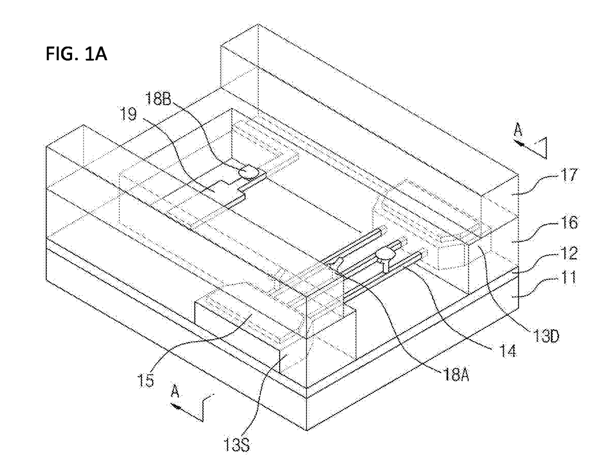
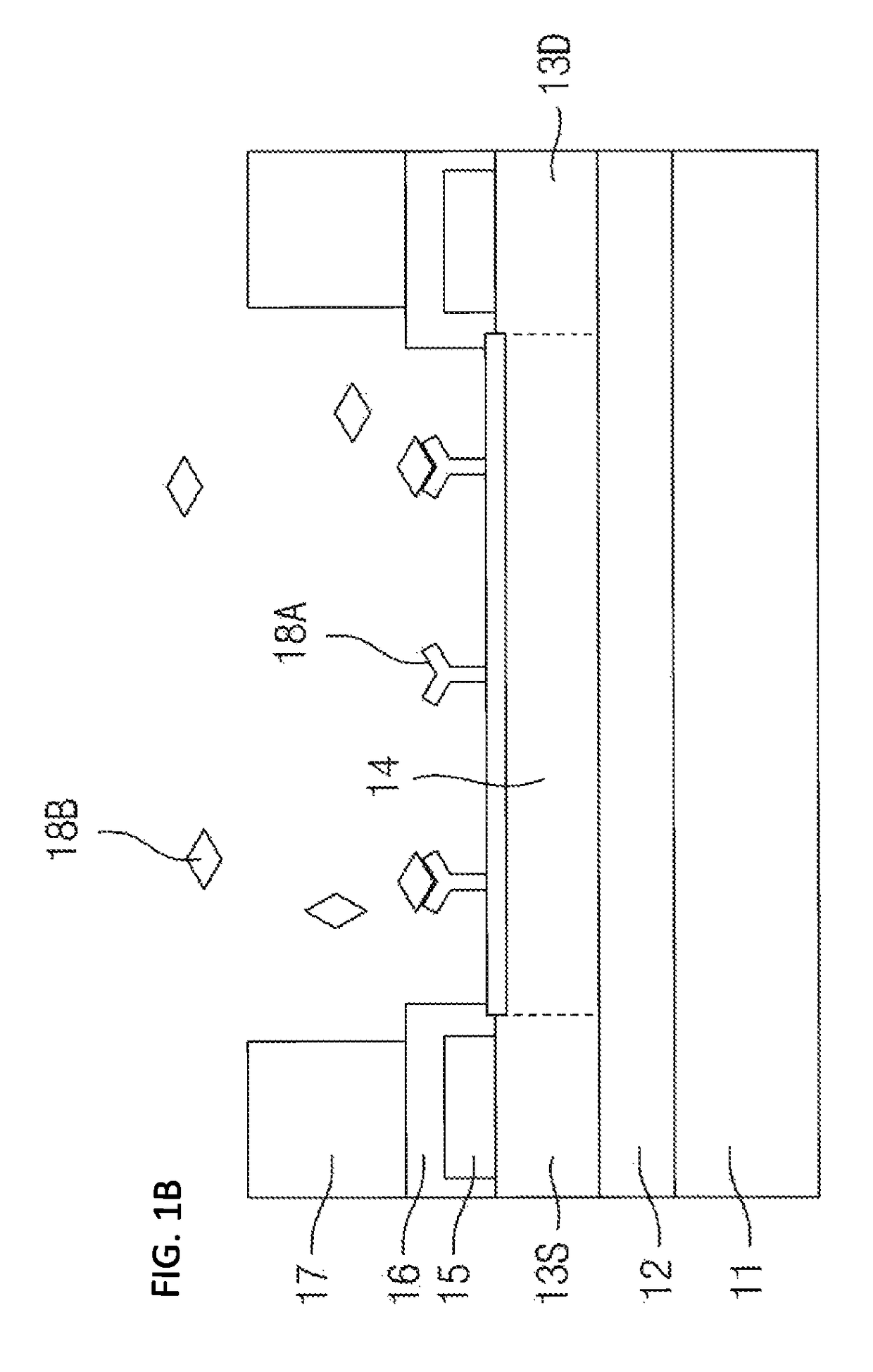
To form the one-dimensional nanowires as described above, an element is fabricated on the expensive SOI substrate, and for this reason, the nanowire field-effect sensor has a problem in that it is costly.
In addition, because it is impossible to reuse a receptor material and a target material, which are used for detection in the nanowire field-effect sensor that is a biosensor, the nanowire field-effect sensor according to the prior art has a problem in that many maintenance costs are incurred.
Furthermore, in the case in which nanowires equal or similar to those used in the nanowire field-effect sensor according to the prior art are used, the sensitivity of the sensor itself is very high, but there is a shortcoming in that the area of the nanowire is very small (several square nanometers to several square microns), and thus the amount of target material that is transferred from the buffer solution to the detection surface is necessarily very limited, indicating that the sensor has low sensitivity.
In the case of the bottom-up method, nanowires formed using a semiconductor processing technique such as CVD (chemical vapor deposition) are arranged at specific positions to thereby fabricate a sensor, and thus the synthesis and arrangement of the nanowires are not easy, making it difficult to produce the sensor in large amounts.

Method used


Image

  • Nanowire field-effect sensor including nanowires having network structure and fabrication method thereof
  • Nanowire field-effect sensor including nanowires having network structure and fabrication method thereof
  • Nanowire field-effect sensor including nanowires having network structure and fabrication method thereof

Examples


Embodiment Construction

[0039]Hereinafter, preferred embodiments of the present invention will be described with reference to the accompanying drawings.

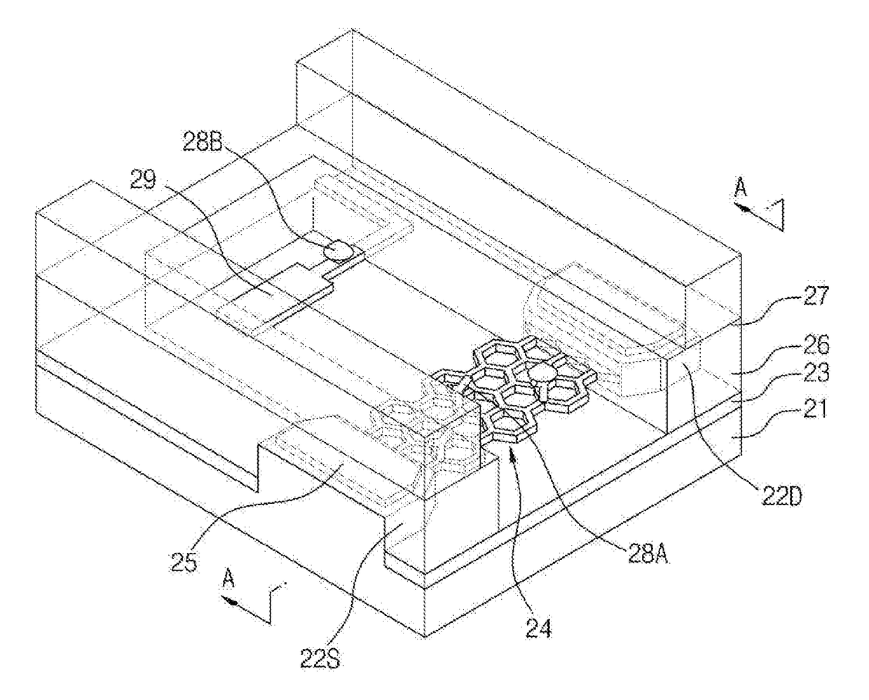
[0040]FIG. 2A illustrates the structure of a nanowire field-effect sensor according to an embodiment of the present invention, and FIG. 2B is a cross-sectional view taken along line A-A of FIG. 2A.

[0041]Referring to FIGS. 2A and 2B, the nanowire field-effect sensor according to the embodiment of the present invention includes: a source electrode region 22S and drain electrode region 22D formed on both sides of a bulk silicon substrate 21 so as to be opposite to each other; a nano-network 24 connected between the source electrode region 22S and the drain electrode region 22D and having a network structure in which a gate insulating layer 24-2 is applied to a pin 24-1 arranged on each sidewall of the network; a bottom insulating layer 23 disposed between the bulk silicon substrate 21 and the nano-network 24 so as to insulate the nano-network 24 from the bulk ...


PUM

PropertyMeasurementUnit
widthaaaaaaaaaa
heightaaaaaaaaaa
sizeaaaaaaaaaa

Abstract

Disclosed herein is a technology for fabricating a nanowire field-effect sensor, in which a bulk silicon substrate is used so that the fabrication cost of the sensor can be reduced while the integration density of the sensor can be increased. In addition, the nanowire field-effect sensor includes a nano-network having a network structure in which pins are vertically arranged on the sidewalls of the network, respectively, and a gate insulating layer is applied to the pins. Due to this nano-network, the detection area of the sensor can be increased to increase its sensitivity, and the structural stability of the sensor can be ensured.

Description

BACKGROUND OF THE INVENTION[0001]Field of the Invention[0002]The present invention relates to a technology for fabricating a nanowire field-effect sensor, and more particularly, to a nanowire field-effect sensor including nanowires having a network structure and to a fabrication method, in which a bulk silicon substrate is used so that the fabrication cost of the sensor can be reduced and the integration density of the sensor can be increased, and a nano-network is effectively insulated so that the high sensitivity and structural stability of the sensor can be ensured.[0003]Description of the Prior Art[0004]An electrochemical sensor is a device that converts a physical or biochemical signal from a target material to be detected into an electrical signal, and is characterized by having a small size and a high detection speed, compared to conventional fluorescent sensors. Such electrochemical sensors are expected to be widely used in applications, including biosensors, chemical sensor...

Claims


Application Information

Patent Timeline
Patent Type & Authority Patents(United States)
IPC IPC(8): G01N27/414H01L21/265H01L29/06H01L29/423
CPCG01N27/4146H01L21/26513H01L29/0649H01L29/0673H01L29/42356H01L29/42364H01L21/02236H01L21/31116
Inventor LEE, JEONG SOOPARK, CHAN OHKIM, DONG HOONKIM, KI HYUN
Owner POSTECH ACAD IND FOUND
Learn More