Adjusting device of an output voltage of a switch power supply, an adjusting method thereof and an integrated chip
a technology of output voltage and switch power supply, which is applied in the direction of power conversion systems, dc-dc conversion, instruments, etc., can solve the problems of blocking the improvement of productivity, easy burnout, and automatic shut down of the computer system, so as to save manpower on product manufacturing, enhance productivity, and enhance the effect of adjusting the output voltage precision
- Summary
- Abstract
- Description
- Claims
- Application Information
AI Technical Summary
Benefits of technology
Problems solved by technology
Method used
Image
Examples
first embodiment
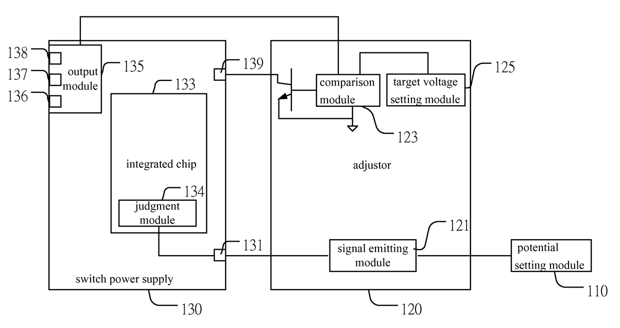
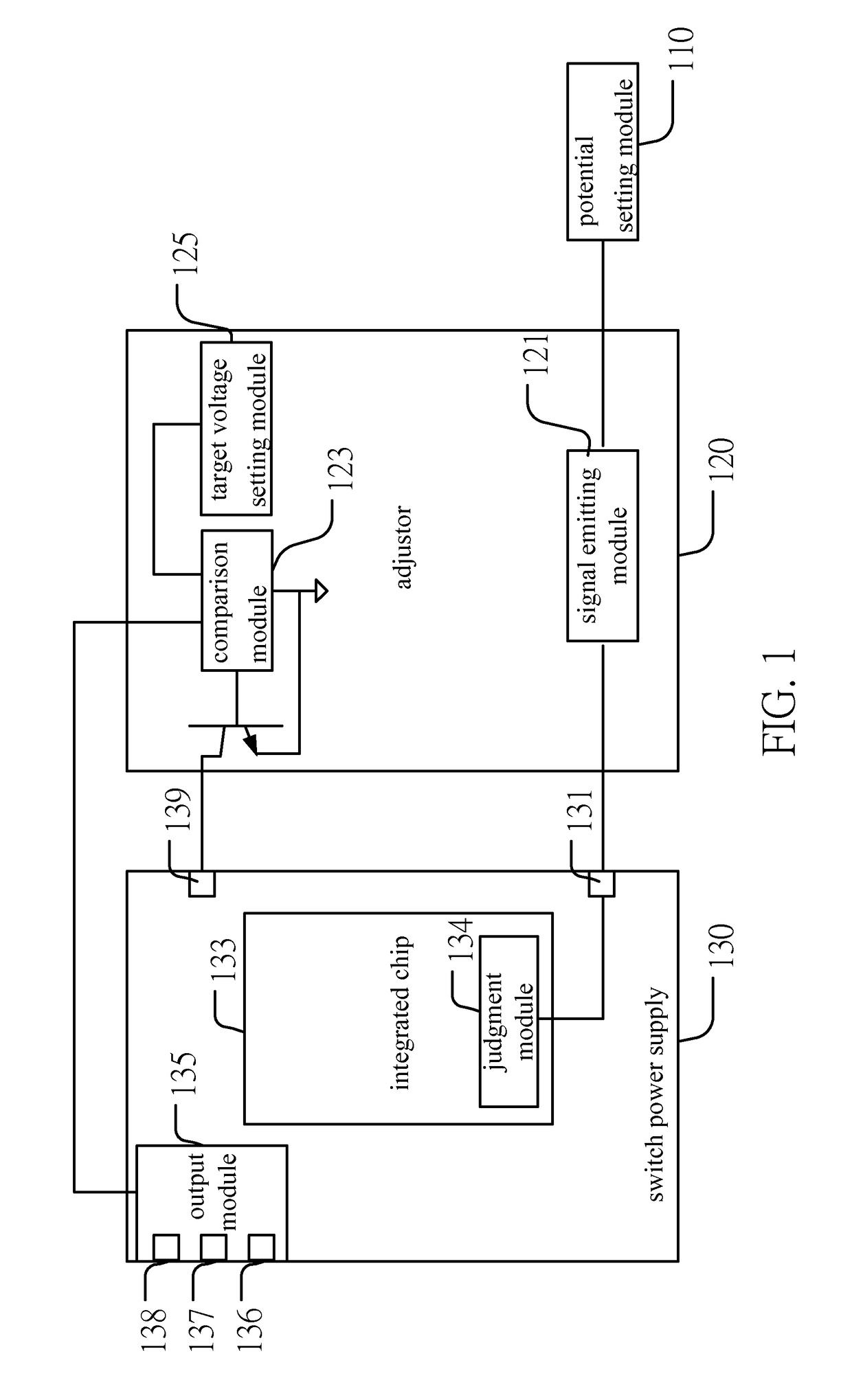
[0084]In the present invention, the potential setting module is disposed in the ATE, the adjustor is a testing tool, and the integrated chip (namely the protection control chip) is a DWA100N-A chip, which integrates the digital variable resistor. The preset voltage of the switch power supply is 12V. The input port of the switch power supply is a PSNONB port, which is connected to a fourth pin of the integrated chip shown in FIG. 3. The switch port is a PG0 port, which is connected to an eighteenth pin of the integrated chip shown in FIG. 3. The first output port of the output module of the switch power supply is connected to a thirteenth pin of the integrated chip shown in FIG. 3 and is electrically connected to the comparison module of the testing tool.
[0085]Referring to FIG. 5, a step S501 is setting the preset voltage of the switch power supply in the target voltage setting module of the adjustor.
[0086]Here, the preset voltage is 12V.
[0087]A step S503 is generating the high level...
second embodiment
[0105]In the present invention, the potential setting module is disposed in the ATE, the adjustor is a testing tool, and the integrated chip (namely the housekeeping chip) is a DWA100N-A chip, which integrates the digital variable resistor. The preset voltage of the switch power supply is 5V. The input port of the switch power supply is a PSNONB port, which is connected to a fourth pin of the integrated chip shown in FIG. 3. The switch port is a PG0 port, which is connected to an eighteenth pin of the integrated chip shown in FIG. 3. The second output port of the output module of the switch power supply is connected to a sixteenth pin of the integrated chip shown in FIG. 3 and is electrically connected to the comparison module of the adjustor.
[0106]Referring to FIG. 6, a step S601 is setting the preset voltage of the switch power supply in the target voltage setting module of the adjustor.
[0107]Here, the preset voltage is 5V. The adjustor directly generates the pulse drive signal.
[0...
PUM
 Abstract
Description
Claims
Application Information
 - R&D
- Intellectual Property
- Life Sciences
- Materials
- Tech Scout
- Unparalleled Data Quality
- Higher Quality Content
- 60% Fewer Hallucinations
Browse by: Latest US Patents, China's latest patents, Technical Efficacy Thesaurus, Application Domain, Technology Topic, Popular Technical Reports.
© 2025 PatSnap. All rights reserved.Legal|Privacy policy|Modern Slavery Act Transparency Statement|Sitemap|About US| Contact US: help@patsnap.com


