Semiconductor device with variable resistance switch and programming method therefor
a technology of variable resistance switch and semiconductor device, which is applied in the direction of power consumption reduction, pulse technique, instruments, etc., can solve the problems of low area efficiency and large power consumption, and achieve the effect of high reliability
- Summary
- Abstract
- Description
- Claims
- Application Information
AI Technical Summary
Benefits of technology
Problems solved by technology
Method used
Image
Examples
first exemplary embodiment
[0056]A first exemplary embodiment of the present invention will be described. FIG. 3 is a figure showing an example of a configuration of a semiconductor device according to the first exemplary embodiment. The semiconductor device includes a first wiring 101, a second wiring 102, a first switch element 103, a second switch element 104, a first selection switch element 106, a second selection switch element 107, a first programming driver 108, and a second programming driver 109. The first wiring 101 and the second wiring 102 are arranged in directions that intersect with each other in a planar view for example, in directions that intersect with each other at a right angle in a planar view or the like. The first switch element 103 and the second switch element 104 are connected in series and arranged at an intersection point of the first wiring 101 and the second wiring 102. Here, one terminal of the first switch element 103 is connected to the first wiring 101. One terminal of the ...
second exemplary embodiment
[0063]As shown in FIG. 5, this exemplary embodiment discloses a structure in which a plurality of the unit elements 110 disclosed in the first exemplary embodiment are arranged in an array shape. Although not clearly specified in the first exemplary embodiment, in this exemplary embodiment, first decode signal lines 121 and second decode signal lines 122 are provided. In order to program the arbitrary unit element 110, the first decode signal line 121 and the second decode signal line 122 control a conduction / non-conduction state of the first selection switch element 106 and the second selection switch element 107. The first decode signal line 121 and the first wiring 101 are arranged in parallel and the second decode signal line 122 and the second wiring 102 are arranged in parallel. A plurality of the first selection switch elements 106 are commonly connected to the first programming driver 108. A plurality of the second selection switch elements 107 are commonly connected to the ...
third exemplary embodiment
[0068]In this exemplary embodiment, the intermediate node 105 of the unit element 110 is used for the programming of the unit element 110 and whereby, this exemplary embodiment further has an effect in which the voltage Vset can be reduced and a possibility of the erroneous writing can be reduced.
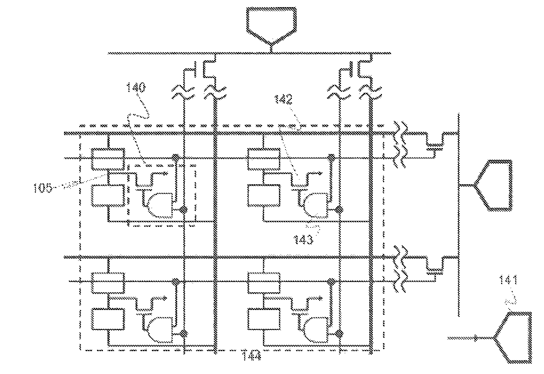
[0069]FIG. 7 shows an example of a configuration of a semiconductor device according to a third exemplary embodiment. This exemplary embodiment discloses a mode in which an intermediate node programming driver 141 is connected to the intermediate node 105 of the unit element 110 via an intermediate node selection circuit 140. Further, the description of the element explained in the exemplary embodiments 1 and 2 will be omitted.
[0070]In FIG. 7, the intermediate node selection circuit 140 is composed of an intermediate node selection switch element 142 and a decode circuit 143. The intermediate node selection switch element 142 changes a state of a connection between the intermediate node 105...
PUM
 Abstract
Description
Claims
Application Information
 - R&D
- Intellectual Property
- Life Sciences
- Materials
- Tech Scout
- Unparalleled Data Quality
- Higher Quality Content
- 60% Fewer Hallucinations
Browse by: Latest US Patents, China's latest patents, Technical Efficacy Thesaurus, Application Domain, Technology Topic, Popular Technical Reports.
© 2025 PatSnap. All rights reserved.Legal|Privacy policy|Modern Slavery Act Transparency Statement|Sitemap|About US| Contact US: help@patsnap.com


