
Selective etch for silicon films

a selective etching and silicon film technology, applied in the direction of electrical appliances, decorative surface effects, decorative arts, etc., can solve the problem of not readily etching silicon, and achieve the effect of less oxygen and more rapid removal

Active Publication Date: 2016-04-26
APPLIED MATERIALS INC
View PDF1156 Cites 147 Cited by
  • Summary
  • Abstract
  • Description
  • Claims
  • Application Information

AI Technical Summary

Problems solved by technology

The Siconi™ etch is largely conformal and selective towards silicon oxide layers but does not readily etch silicon regardless of whether the silicon is amorphous, crystalline or polycrystalline.

Method used


Image

  • Selective etch for silicon films
  • Selective etch for silicon films
  • Selective etch for silicon films

Examples


Embodiment Construction

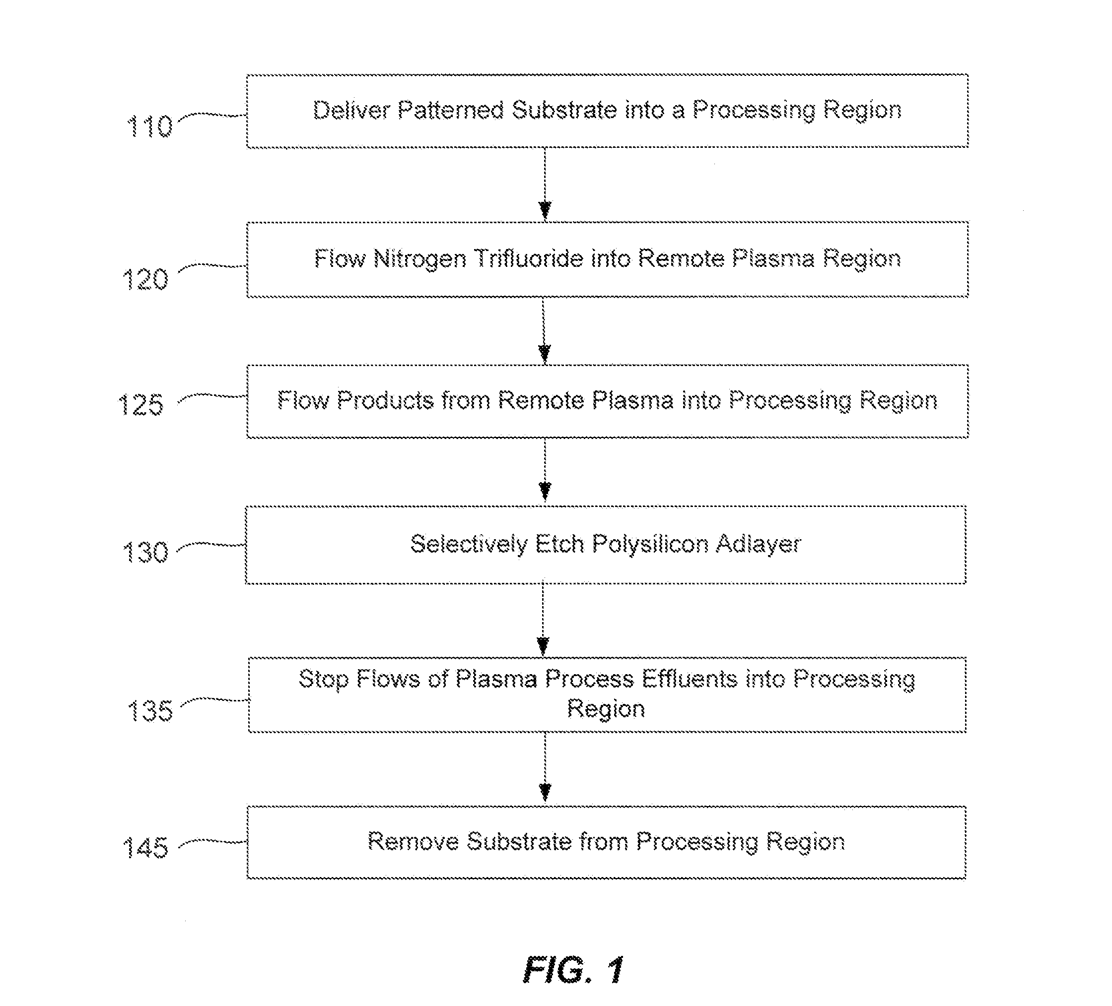
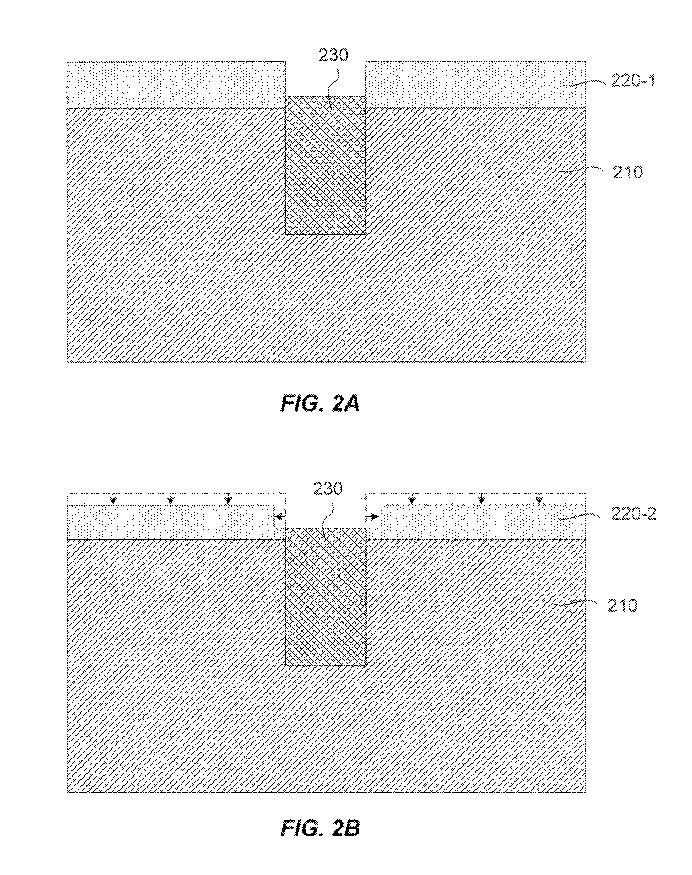
[0018]A method of etching patterned heterogeneous silicon-containing structures is described and includes a remote plasma etch with inverted selectivity compared to existing remote plasma etches. The methods may be used to conformally trim polysilicon while removing little or no silicon oxide. More generally, silicon-containing films containing less oxygen are removed more rapidly than silicon-containing films which contain more oxygen. Other exemplary applications include trimming silicon carbon nitride films while essentially retaining silicon oxycarbide. Applications such as these are enabled by the methods presented herein and enable new process flows. These process flows are expected to become desirable for a variety of finer linewidth structures. Methods contained herein may also be used to etch silicon-containing films faster than nitrogen-and-silicon containing films having a greater concentration of nitrogen.

[0019]Siconi™ etch processes have used a hydrogen source of ammoni...


PUM

PropertyMeasurementUnit
partial pressureaaaaaaaaaa

Abstract

A method of etching patterned heterogeneous silicon-containing structures is described and includes a remote plasma etch with inverted selectivity compared to existing remote plasma etches. The methods may be used to conformally trim polysilicon while removing little or no silicon oxide. More generally, silicon-containing films containing less oxygen are removed more rapidly than silicon-containing films which contain more oxygen. Other exemplary applications include trimming silicon carbon nitride films while essentially retaining silicon oxycarbide. Applications such as these are enabled by the methods presented herein and enable new process flows. These process flows are expected to become desirable for a variety of finer linewidth structures. Methods contained herein may also be used to etch silicon-containing films faster than nitrogen-and-silicon containing films having a greater concentration of nitrogen.

Description

CROSS REFERENCE TO RELATED APPLICATIONS[0001]This application is a nonprovisional of, and claims the benefit of the filing date of U.S. Provisional Patent Application No. 61 / 348,920, filed May 27, 2010, entitled “OXIDE DESELECTIVE ETCH” by Jingchun Zhang et al., the entire disclosure of which is incorporated herein by reference for all purposes.BACKGROUND OF THE INVENTION[0002]Integrated circuits are made possible by processes which produce intricately patterned material layers on substrate surfaces. Producing patterned material on a substrate requires controlled methods for removal of exposed material. Chemical etching is used for a variety of purposes including transferring a pattern in photoresist into underlying layers, thinning layers or thinning lateral dimensions of features already present on the surface. Often it is desirable to have an etch process which etches one material faster than another helping e.g. a pattern transfer process proceed. Such an etch process is said to...

Claims


Application Information

Patent Timeline
Patent Type & Authority Patents(United States)
IPC IPC(8): H01L21/302H01L21/311H01L21/3065C23F1/00C23F3/00H01L21/3213H01L21/461B44C1/22C03C15/00C03C25/68
CPCH01L21/31116H01L21/32137H01L21/3065H01L21/311H01L21/32136
Inventor ZHANG, JINGCHUNWANG, ANCHUANINGLE, NITIN K.
Owner APPLIED MATERIALS INC
Learn More