High impedance resistor device applied in high voltage environment
- Summary
- Abstract
- Description
- Claims
- Application Information
AI Technical Summary
Benefits of technology
Problems solved by technology
Method used
Image
Examples
Embodiment Construction
[0026]The following description is about embodiments of the present invention; however it is not intended to limit the scope of the present invention.
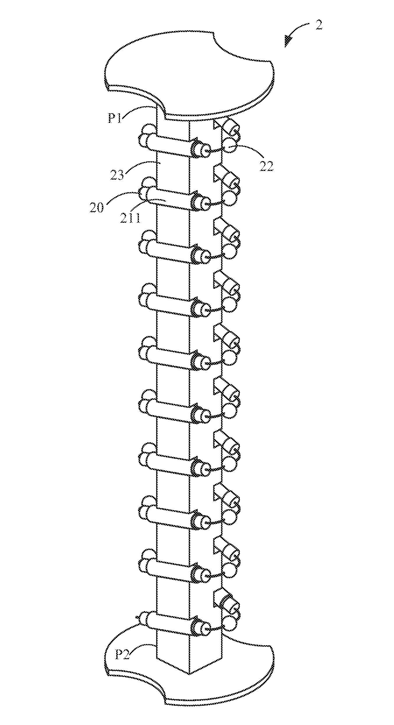
[0027]FIG. 2 shows a structure diagram of high impedance resistor 20 of present application. The body of the high impedance resistor 20 encases an insulation cover 211. In the prior art, the connecting portion of connected resistors tends to have a tip-shape welding point caused by the bad welding technique. To avoid point discharge phenomena by the tip-shape welding point, present application provides pellet connector 22 configured at the connected portion to cover the welding point.
[0028]FIG. 3 shows a cross-section of high impedance resistor device 20 applied in high voltage environment. The cross-section shape of voltage-endurance column 23 is a square shape. And the neighbored high impedance resistors 20 are configured at the two opposite surface of the voltage-endurance column 23 respectively.
[0029]FIG. 4 shows the high impedance...
PUM
 Abstract
Description
Claims
Application Information
 - R&D
- Intellectual Property
- Life Sciences
- Materials
- Tech Scout
- Unparalleled Data Quality
- Higher Quality Content
- 60% Fewer Hallucinations
Browse by: Latest US Patents, China's latest patents, Technical Efficacy Thesaurus, Application Domain, Technology Topic, Popular Technical Reports.
© 2025 PatSnap. All rights reserved.Legal|Privacy policy|Modern Slavery Act Transparency Statement|Sitemap|About US| Contact US: help@patsnap.com


