Hard-material-coated bodies composed of metal, cemented hard material, cermet or ceramic and processes for producing such bodies
a cemented hard material and hard-material coating technology, applied in the direction of superimposed coating process, coating, chemical vapor deposition coating, etc., can solve the problems of inability to use, inadequacies, low hardness,
- Summary
- Abstract
- Description
- Claims
- Application Information
AI Technical Summary
Benefits of technology
Problems solved by technology
Method used
Image
Examples
example 1
[0029]On WC / Co hard-metal indexable inserts precoated with a 5 μm thick TiN / TiCN / TiN coating system, there is deposited a TiSiCN nanocomposite coating as the top coating by means of the thermal CVD process according to the invention.
[0030]For this purpose a gas mixture of 4.2 mL / min TiCl4, 20.4 mL / min SiCl4, 7.9 mL / min acetonitrile (CH3CN) and 2400 mL / min hydrogen is passed at 800° C. and 6 kPa into a horizontal hot-wall CVD reactor with an inside diameter of 75 mm for the deposition of the TiSiCN nanocomposite coating.
[0031]After a coating time of 120 min, a gray coating, which has a coating thickness of 4.3 μm, is apparent.
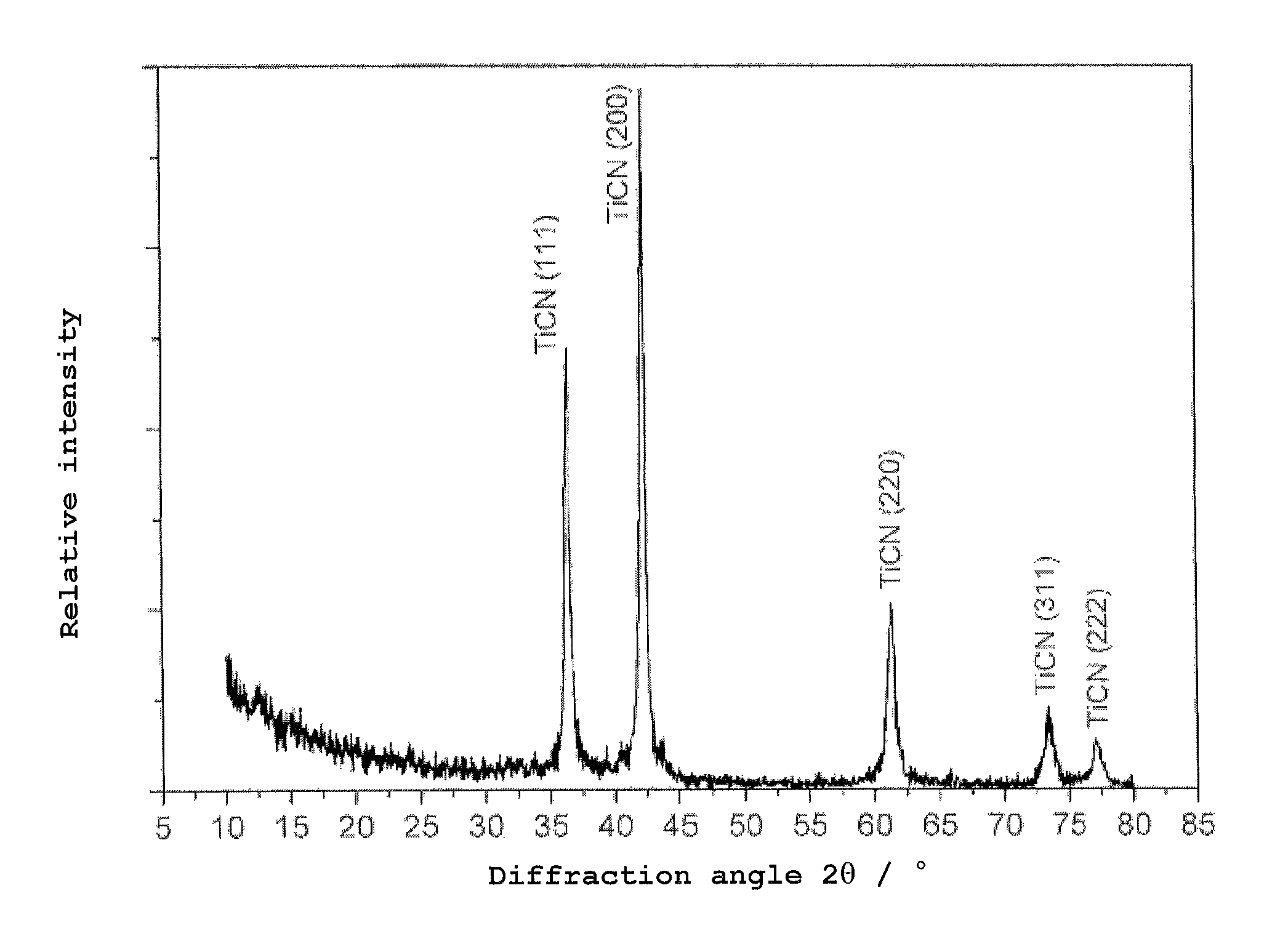
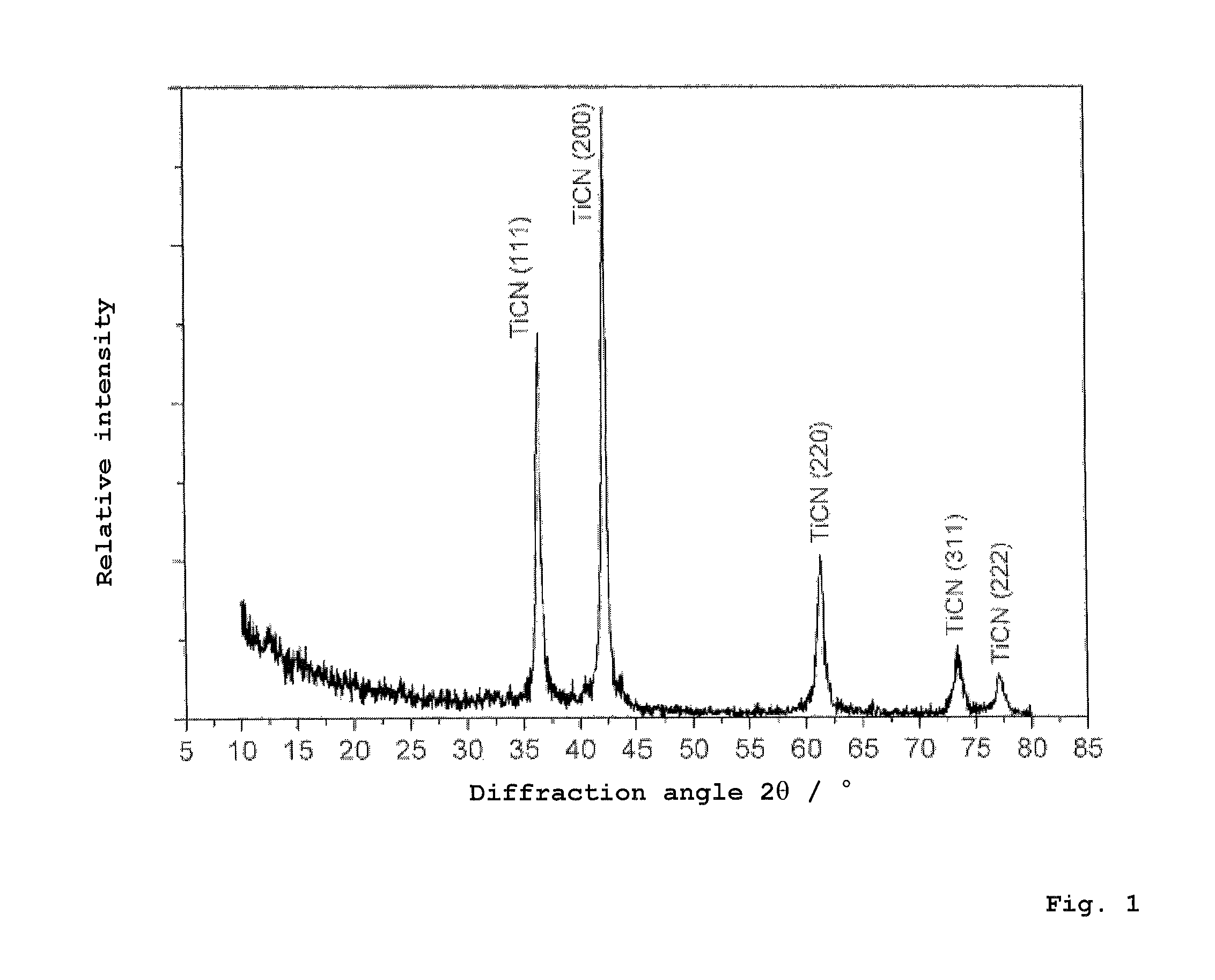
[0032]In the radiographic thin-film analysis performed at grazing incidence, only the crystalline TiCxN1-x is found (see x-ray diffraction diagram in FIG. 1). Silicon is contained in a second, amorphous SiCxNy phase, by analogy with the XPS analysis performed in Example 3. The mean grain size of the nanocrystalline phase of the TiCxN1-x was determined to be 19±0...
example 2
[0041]On a WC / Co indexable insert precoated with 1 μm TiN and 3 μm TiCN, there is first applied a further TiN coating with a thickness of 0.5 μm, followed by the TiSiCN nanocomposite coating according to the invention.
[0042]For this purpose a gas mixture of 8.3 mL / min TiCl4, 10 mL / min Si2Cl6, 10.6 mL / min CH3CN and 2400 mL / min hydrogen is passed at 850° C. and 6 kPa into the CVD reactor mentioned in Example 1. After a coating time of 90 min, a gray coating, which has a coating thickness of 7.6 μm, is obtained.
[0043]In the radiographic thin-film analysis performed at grazing incidence, only the crystalline TiCxN1-x is found, just as in Example 1. Silicon is contained in a second, amorphous SiCxNy phase, by analogy with the XPS analysis performed in Example 3. By means of Rietveld analysis, a mean grain size of 39±2 nm was obtained for the nanocrystalline TiCxN1-x phase.
[0044]The WDX analysis yielded the following elemental contents:[0045]41.70 atomic % Ti,[0046]4.30 atomic % Si,[0047]...
example 3
[0052]On a WC / Co indexable insert precoated with 3 μm TiN, there is first applied a further TiN coating with a thickness of 0.5 μm, followed by the nanocomposite coating of TiSiCN according to the invention.
[0053]For this purpose a gas mixture of 4.2 mL / min TiCl4, 10 mL / min Si2Cl6, 10.6 mL / min CH3CN and 2400 mL / min hydrogen is passed at 850° C. and 6 kPa into the CVD reactor mentioned in Example 1. After a coating time of 90 min, a gray coating, which has a coating thickness of 3.5 μm, was deposited.
[0054]In the radiographic thin-film analysis performed at grazing incidence, only the crystalline TiCxN1-x is found, just as in Example 1. A crystalline silicon-containing phase is not radiographically detectable. By XPS analysis of the TiSiCN coating, however, Si—N bonds were clearly detected at 101.8 eV and Si—C bonds at 100.7 eV after evaluation of the Si2p spectrum, which bonds indicate the presence of an amorphous SiCxNy phase.
[0055]The mean grain size of the nanocrystalline phase o...
PUM
| Property | Measurement | Unit |
|---|---|---|
| crystallite size | aaaaa | aaaaa |
| crystallite size | aaaaa | aaaaa |
| temperatures | aaaaa | aaaaa |
Abstract
Description
Claims
Application Information
 - R&D
- Intellectual Property
- Life Sciences
- Materials
- Tech Scout
- Unparalleled Data Quality
- Higher Quality Content
- 60% Fewer Hallucinations
Browse by: Latest US Patents, China's latest patents, Technical Efficacy Thesaurus, Application Domain, Technology Topic, Popular Technical Reports.
© 2025 PatSnap. All rights reserved.Legal|Privacy policy|Modern Slavery Act Transparency Statement|Sitemap|About US| Contact US: help@patsnap.com


