Electronic device for implementing digital functions through molecular functional elements

a technology of molecular functional elements and electronic devices, applied in pulse generators, instruments, pulse techniques, etc., can solve the problems of nano-electronic “transistor-like” solutions that are difficult to achieve, the cost and feasibility of lithographic processes on scales smaller than the current ones are problematic, and the effect of reasonable cost and high performan

Active Publication Date: 2016-02-09
DHITECH DISTRETTO TECHCO HIGH TECH S C A R L
View PDF3 Cites 2 Cited by
  • Summary
  • Abstract
  • Description
  • Claims
  • Application Information

AI Technical Summary

Benefits of technology

[0020]Particularly, an electronic device is proposed, that is based on physical quantum phenomena, while allowing the integration of several functional elements, such as to compose a processor or a complex logic network, and which can be manufactured at reasonable costs and provide high performance.

Problems solved by technology

However, such technological evolution seems to be reaching its limit.
Costs and feasibility of lithographic processes on scales that are smaller than the current ones appear to be problematic.
However, nano-electronic “transistor-like” solutions have severe drawbacks, since to date they do not allow obtaining the same performance of the state-of-the-art micro-electronic transistors.
Furthermore, a transistor-based system includes complex interconnections, which are obtained by lithographic processes, thus not allowing overcoming the above-mentioned limitations of such lithographic processes.
However, to date, QCAs did not prove to be capable of implementing complex processors, since the implementation of prior art complex QCA cell processors use substantially conventional lithographic processes, to the extent of the spatial resolution of a single QCA cell, with all the above-mentioned limitations thereof.
A further drawback of prior art QCA solutions, particularly at a molecular scale, is that they are implemented on the basis of molecules that are highly symmetrical in structure and electric configuration, while real molecules tend to be asymmetric, at least due to the deposition thereof on substrates, together with other possibly similar molecules.
The use of not exactly symmetric molecules is a severe limitation on the performance that can be obtained by QCAs.
From what has been stated above, it shall be apparent that the desire to provide nano-electronic integrated devices with digital processing performance comparable to those of current micro-electronic circuits and processors, and at a reasonable cost, is largely unmet.

Method used


Image

  • Electronic device for implementing digital functions through molecular functional elements
  • Electronic device for implementing digital functions through molecular functional elements
  • Electronic device for implementing digital functions through molecular functional elements

Examples


Embodiment Construction

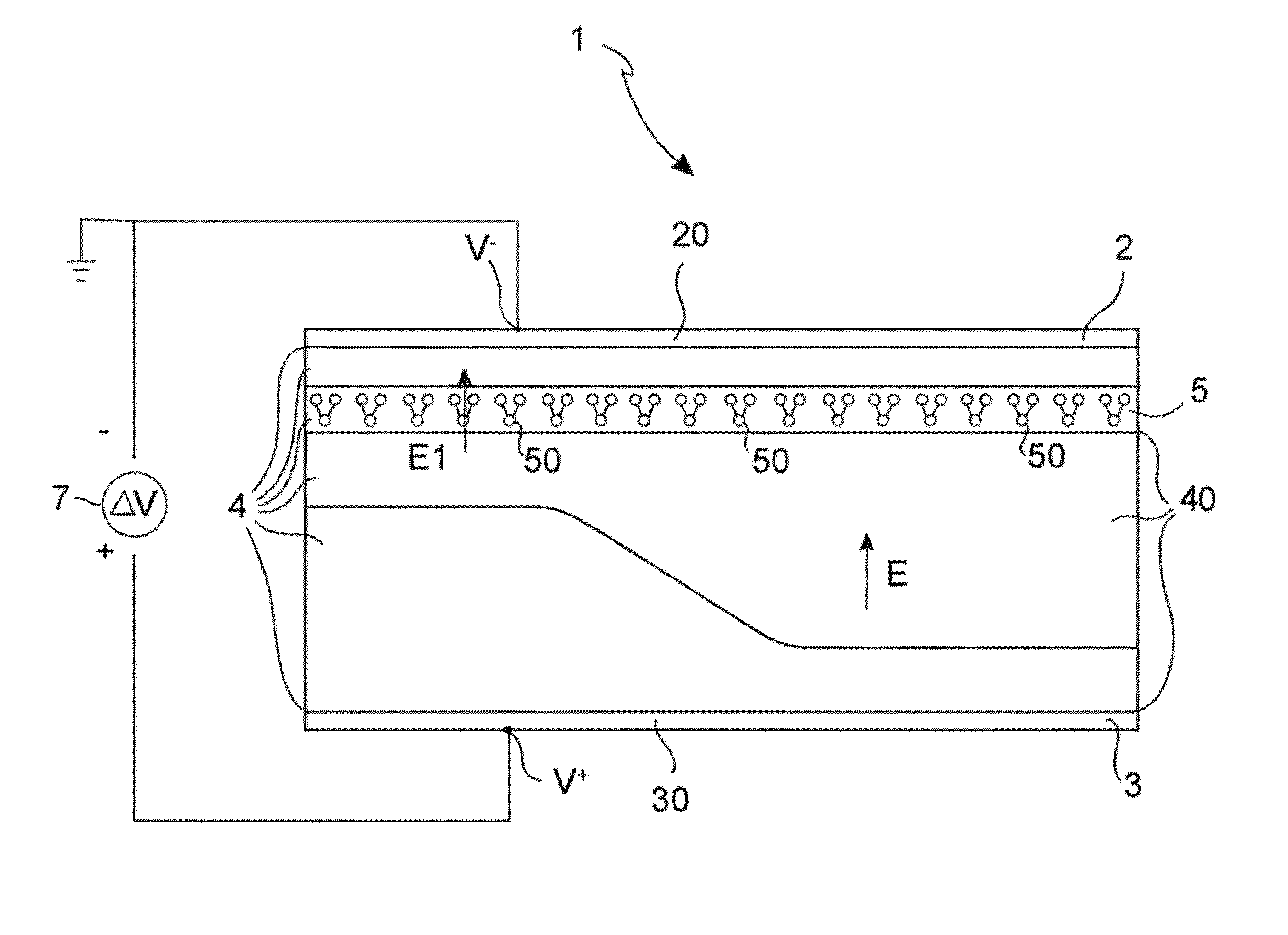
[0046]With reference to FIG. 1, an electronic device 1 for implementing digital functions will be now described, according to a preferred embodiment of the disclosure.

[0047]As shown in the sectional view of FIG. 1, the electronic device comprises: a first electrode region 2 and a second electrode region 3, separated by an interposing region 4 comprising a dielectric region 40. The first 2 and second 3 electrode regions comprise at least one first electrode 20 and at least one second electrode 30, respectively, which are configured to generate an electrode electric field E in the interposing region 4 (particularly, at each point of the interposing region 4) depending on an electric potential difference ΔV applied to the first and second electrodes.

[0048]In FIG. 1, such a potential difference ΔV corresponds to the difference between the potentials V+ and V− applied by a source 7 (for example, a voltage generator 7) to the second electrode 30 and the first electrode 20, respectively.

[0...


PUM


Abstract

An electronic device for implementing digital functions comprising a first and a second electrode regions, separated by an interposing region comprising a dielectric region, is described. The first and the second electrode regions comprise at least one first electrode and at least one second electrode, respectively, configured to generate in the interposing region an electric field depending on an electric potential difference applied thereto. In the interposing region, a molecular layer is comprised, which is composed of a plurality of molecules, each being capable of assuming one or more states, in a controllable manner, depending on a sensed electric field. The dielectric region has a spatially variable dielectric profile, to determine a respective spatially variable field profile of the sensed electric field at the molecular layer.

Description

BACKGROUND[0001]1. Technical Field[0002]The present disclosure relates to an electronic device for implementing digital functions and miniaturized logic gates, based on molecular functional elements, and to a method for digital computation implemented by such a device.[0003]An electronic processing system, employing one or more of the above-mentioned devices, and a method for manufacturing the same device are also within the disclosure.[0004]2. Description of the Related Art[0005]The evolution of microelectronics, particularly applied to processors and electronic computers based on integrated circuits, has developed over the last decades while keeping the extraordinary pace foreseen by the so-called “Moore's Law”. This emerged particularly in the increasingly improved miniaturization of integrated electronic circuits, or in the increasing computational capacity that can be obtained while keeping dimensions constant, which in turn depends on the number of functional elements (for exa...

Claims


Application Information

Patent Timeline
Patent Type & Authority Patents(United States)
IPC IPC(8): H03K12/00H03K19/195H01L51/00G06N99/00H01L49/00B82Y10/00
CPCH03K19/195B82Y10/00G06N99/007H01L49/006H01L51/0098Y10S977/774Y10S977/89Y10S977/933H10N99/05H10K30/671B82Y40/00H01L27/11803
Inventor BRAMANTI, ALESSANDRO, PAOLO
Owner DHITECH DISTRETTO TECHCO HIGH TECH S C A R L
Why Eureka
Try Eureka