Junction field effect transistors and associated fabrication methods

a junction field and transistor technology, applied in the field of semiconductor technology, can solve the problems of reduced conductive path width, increased resistance, low gate-source breakdown voltage, etc., and achieve the effects of reducing pinch-off voltage, high gate-source breakdown voltage, and enhancing pinch-off

Active Publication Date: 2016-01-05
CHENGDU MONOLITHIC POWER SYST
View PDF2 Cites 2 Cited by
  • Summary
  • Abstract
  • Description
  • Claims
  • Application Information

AI Technical Summary

Benefits of technology

[0007]The embodiments of the present invention produce new pinch-off region in the JFET by adding a shielding layer to enhance the pinch-off effect. So, the pinch-off voltage is reduced while the distance between the source region and the gate region is maintained. In addition, a high gate-source breakdown voltage and a low on-resistance can be achieved. Thus the design of the JFET can be simple since there does not need a tradeoff in performance.

Problems solved by technology

However, this reduces the width of the conductive path, while increases the on-resistance.
In addition, this also reduces the distance between the source region 104 and the gate region 105 and results in a low gate-source breakdown voltage.
Besides, an optical lithography with higher resolution may be needed and the fabrication process may become more complicated.

Method used


Image

  • Junction field effect transistors and associated fabrication methods
  • Junction field effect transistors and associated fabrication methods
  • Junction field effect transistors and associated fabrication methods

Examples


Embodiment Construction

[0015]Reference will now be made in detail to the preferred embodiments of the invention, examples of which are illustrated in the accompanying drawings. In some instances, well known structures and functions have not been shown or described in detail to avoid unnecessarily obscuring the description of the embodiments of the technology. In some instances, similar structures and functions that have been described in detail for other embodiments are not been described in detail for such embodiments to simplify and make clear understanding of the embodiments. It is intended that the terminology used in the description presented below be interpreted in its broadest reasonable manner, even though it is being used in conjunction with a detailed description of certain embodiments of the technology.

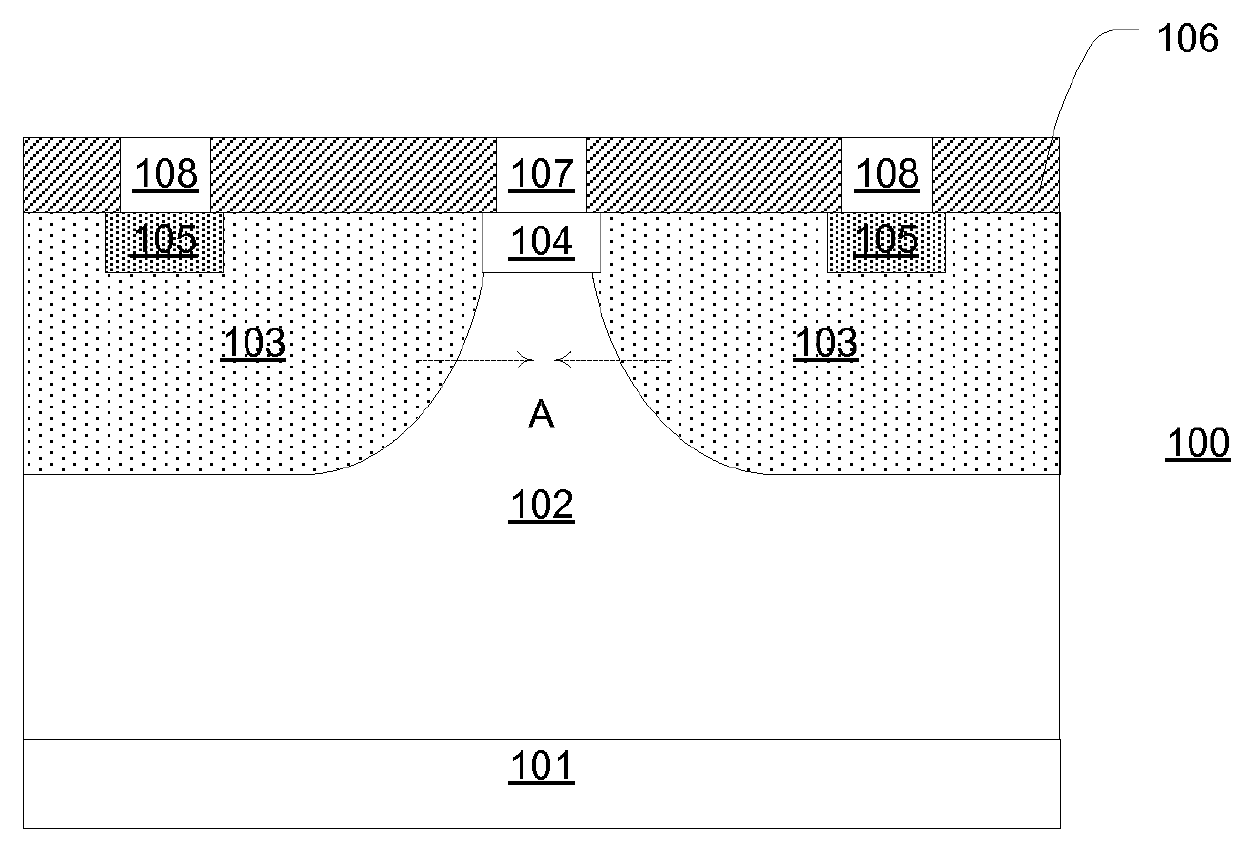
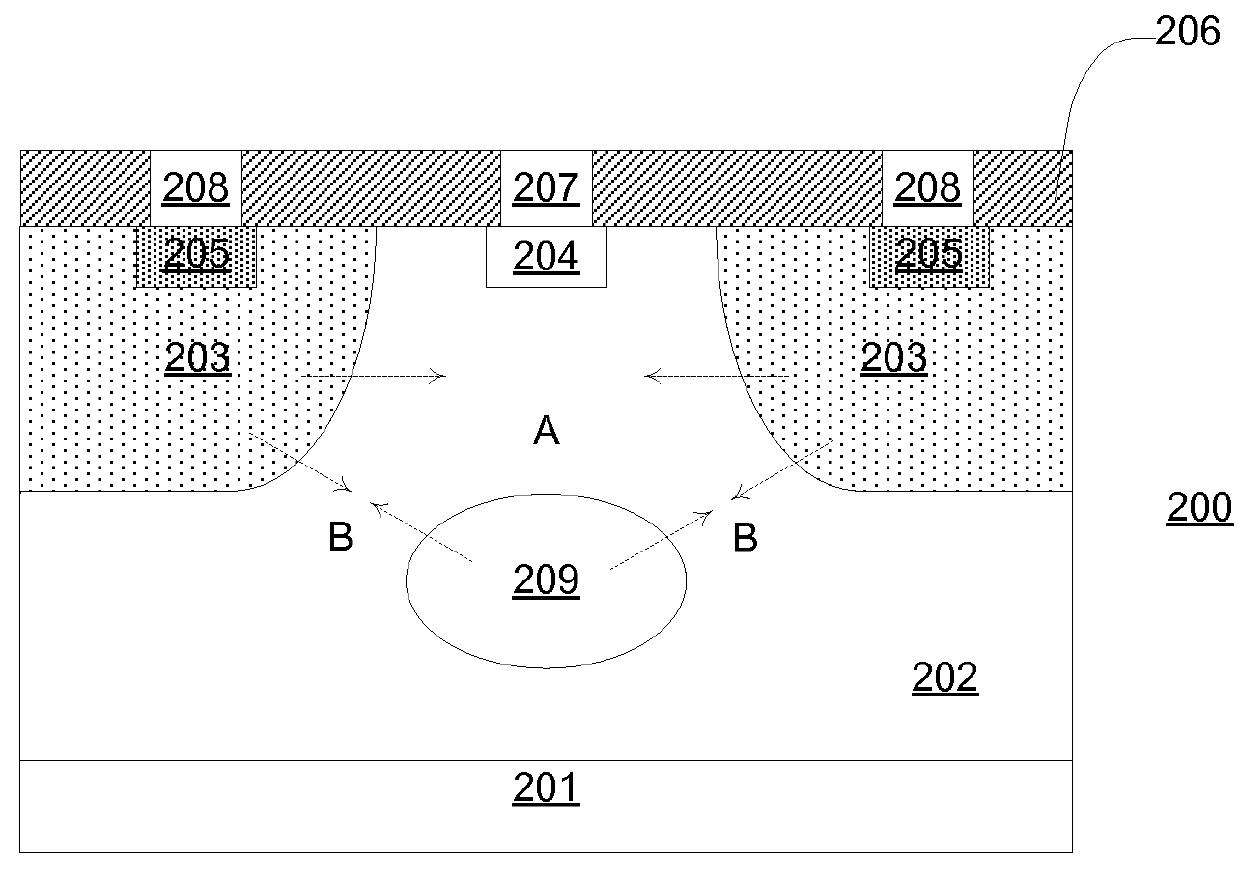
[0016]FIG. 2 illustrates a cross-sectional view of a JFET 200 according to an embodiment of the present invention. The JFET 200 comprises an N+ drain region 201 generally functioning as a semicon...


PUM


Abstract

A JFET having a semiconductor substrate of a first doping type, an epitaxial layer of the first doping type located on the semiconductor substrate, a body region of a second doping type located in the epitaxial layer, a source region of the first doping type located in the epitaxial layer, a gate region of the second doping type located in the body region, and a shielding layer of the second doping type located in the epitaxial layer, wherein the semiconductor substrate is configured as a drain region, the shielding layer is in a conductive path formed between the source region and the drain region.

Description

CROSS-REFERENCE TO RELATED APPLICATION[0001]This application claims the benefit of CN application No. 201210422691.5, field on Oct. 30, 2012, and incorporated herein by reference.TECHNICAL FIELD[0002]The present invention generally relates to semiconductor technology, and more particularly but not exclusively relates to junction field effect transistors and associated fabrication methods.BACKGROUND[0003]FIG. 1 illustrates a cross-sectional view of a prior art N-channel junction field effect transistor (JFET) 100. The JFET is a vertical device and it comprises an N+ drain region 101 (generally as a semiconductor substrate), an N− epitaxial layer 102 located on the N+ drain region 101, a P body region 103 located in the N− epitaxial layer 102, an N+ source region 104 located in the N− epitaxial layer 102 and surrounded by the P body region 103, and a P+ gate region 105 located in the P body region 103. The JFET further comprises an interlayer dielectric layer (ILDL) 106, a source cont...

Claims


Application Information

Patent Timeline
Patent Type & Authority Patents(United States)
IPC IPC(8): H01L27/06H01L27/146H01L27/098
CPCH01L27/0617H01L27/098H01L27/14679H01L27/085H01L29/0619H01L29/0623H01L29/0653H01L29/1066H01L29/1608H01L29/24H01L29/407H01L29/41766H01L29/66712H01L29/66734H01L29/66909H01L29/7802H01L29/7803H01L29/7811H01L29/7813H01L29/7828H01L29/7832H01L29/8083
Inventor MA, RONGYAOLI, TIESHENGZHANG, LEIFU, DAPING
Owner CHENGDU MONOLITHIC POWER SYST
Why Eureka
Try Eureka