Method of mounting devices in substrate and device-mounting substrate structure thereof
a technology of mounting substrate and mounting device, which is applied in the direction of final product manufacturing, sustainable manufacturing/processing, and semiconductor/solid-state device details. it can solve the problems of weak mechanical strength of the portion, difficult to appropriately connect the two conductive layers, and difficult to introduce the plating solution
- Summary
- Abstract
- Description
- Claims
- Application Information
AI Technical Summary
Benefits of technology
Problems solved by technology
Method used
Image

Examples
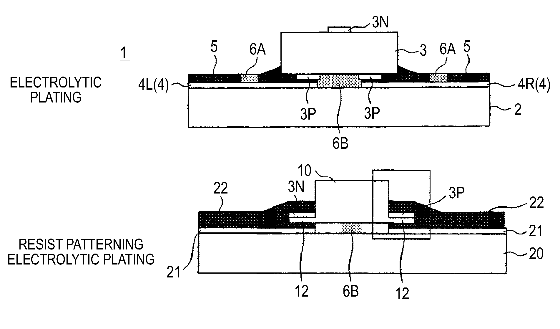
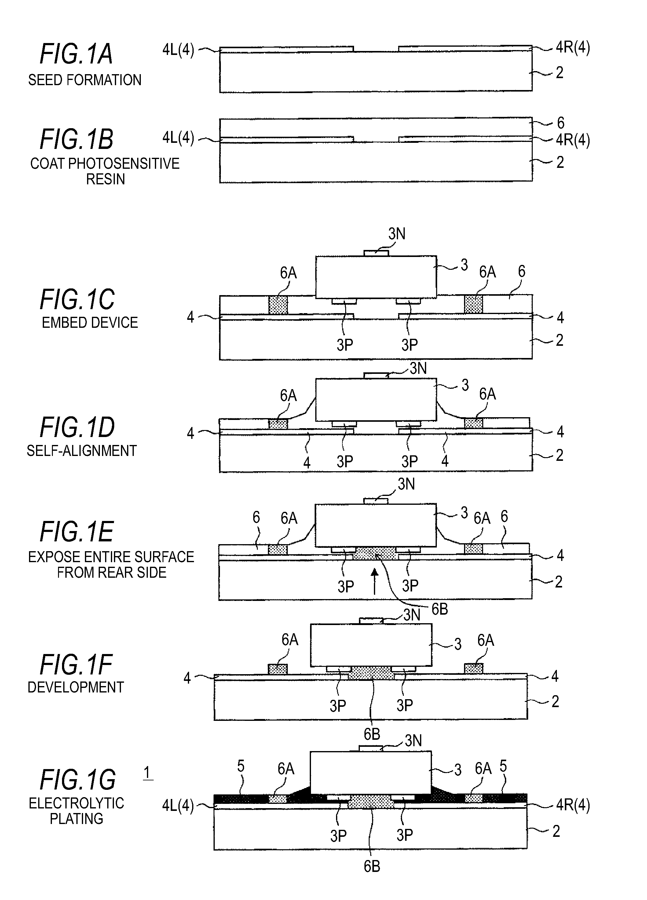
first embodiment
[0095]The LED chip 3B having such a structure is a top emission type in which light is emitted upwardly. In the top emission type, it is not necessary that the temporary fixing portion 6B has transparency or lightfastness. Therefore, it is advantageous that a wide variety of materials can be selected. Such an advantage is common to the
[0096]In addition, since the mounting method itself is common to the previously described embodiment, description thereof will be omitted. In this embodiment, the P-electrode 3P and the N-electrode 3N are positioned in the upward direction from the metal wiring layer 4 to nearly face the metal wiring layer 4 and independently connected to the facing wiring lines 6P and 6N, respectively.
[0097]Therefore, in this connection, electrical connections for both the P and N sides are completed, and electrical connections within the trio chip 1A are completed.
second embodiment
[0098]Another embodiment, according to principles of the present invention(s), relates to a method of mounting in the panel substrate the trio chip (a fundamental unit of the color pixel configuration) in which the internal LED chip 3 can be mounted in the trio substrate 2 using the method of the first or
[0099]FIGS. 4A and 4B are a plan view illustrating the trio chip 10 and a cross-sectional structural diagram illustrating the panel substrate after mounting the trio chip 10, respectively.
[0100]The trio chip 10 shown in FIG. 4A corresponds to an example of the device according to the embodiment of the present invention. In addition, the device denoted by the reference numeral “1” in FIGS. 1A to 1G and the device denoted by the reference number “10” in FIGS. 4A and 4B are similarly called “trio chip.” However, for example, the internal configuration obtained by transparently seeing the internal side of FIG. 4B corresponds to that shown in FIGS. 1A to 1G. Referring to FIG. 4B, since t...
PUM
| Property | Measurement | Unit |
|---|---|---|
| thickness | aaaaa | aaaaa |
| size | aaaaa | aaaaa |
| thickness | aaaaa | aaaaa |
Abstract
Description
Claims
Application Information
 - R&D
- Intellectual Property
- Life Sciences
- Materials
- Tech Scout
- Unparalleled Data Quality
- Higher Quality Content
- 60% Fewer Hallucinations
Browse by: Latest US Patents, China's latest patents, Technical Efficacy Thesaurus, Application Domain, Technology Topic, Popular Technical Reports.
© 2025 PatSnap. All rights reserved.Legal|Privacy policy|Modern Slavery Act Transparency Statement|Sitemap|About US| Contact US: help@patsnap.com