Semiconductor device, related manufacturing method, and related electronic device

a semiconductor device and manufacturing method technology, applied in the direction of fluid speed measurement, semiconductor/solid-state device details, instruments, etc., can solve the problems of unsatisfactory performance of one or more coupled elements, unsatisfactory quality of semiconductor devices and related manufacturing yields, etc., to achieve robust bonding, satisfactory quality of semiconductor devices, and substantially effective vacuum maintenance

Active Publication Date: 2016-05-31
SEMICON MFG INT (SHANGHAI) CORP
View PDF2 Cites 0 Cited by
  • Summary
  • Abstract
  • Description
  • Claims
  • Application Information

AI Technical Summary

Benefits of technology

[0019]According to embodiments of the invention, in semiconductor devices, undesirable coupling between components (e.g., between an inductors and getters) may be minimized or substantially prevented, vacuum may be substantially effectively maintained, and / or substantially robust bonding may be ensured. Advantageously, satisfactory quality of the semiconductor devices and a satisfactory yield of the manufacturing process may be substantially attained.

Problems solved by technology

If the getter is undesirably coupled with another element of the substantially vacuum structure, e.g., through inductive coupling, the performance of one or more of the coupled elements may be unsatisfactory.
As a result, the quality of the semiconductor device and the related manufacturing yield may be unsatisfactory.

Method used


Image

  • Semiconductor device, related manufacturing method, and related electronic device
  • Semiconductor device, related manufacturing method, and related electronic device
  • Semiconductor device, related manufacturing method, and related electronic device

Examples


Embodiment Construction

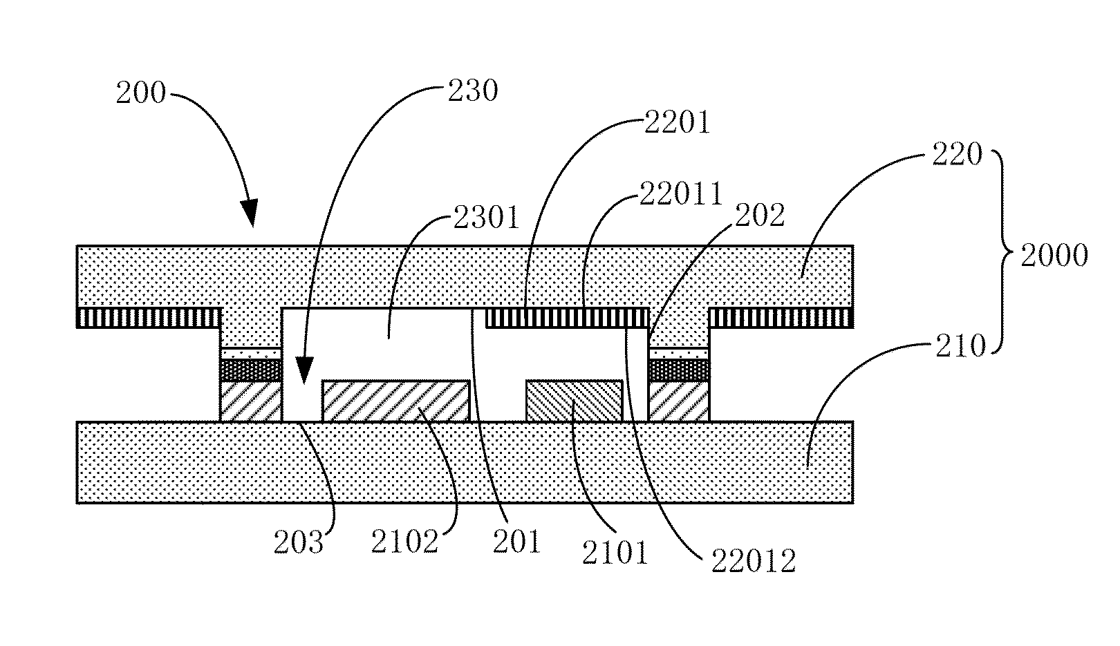
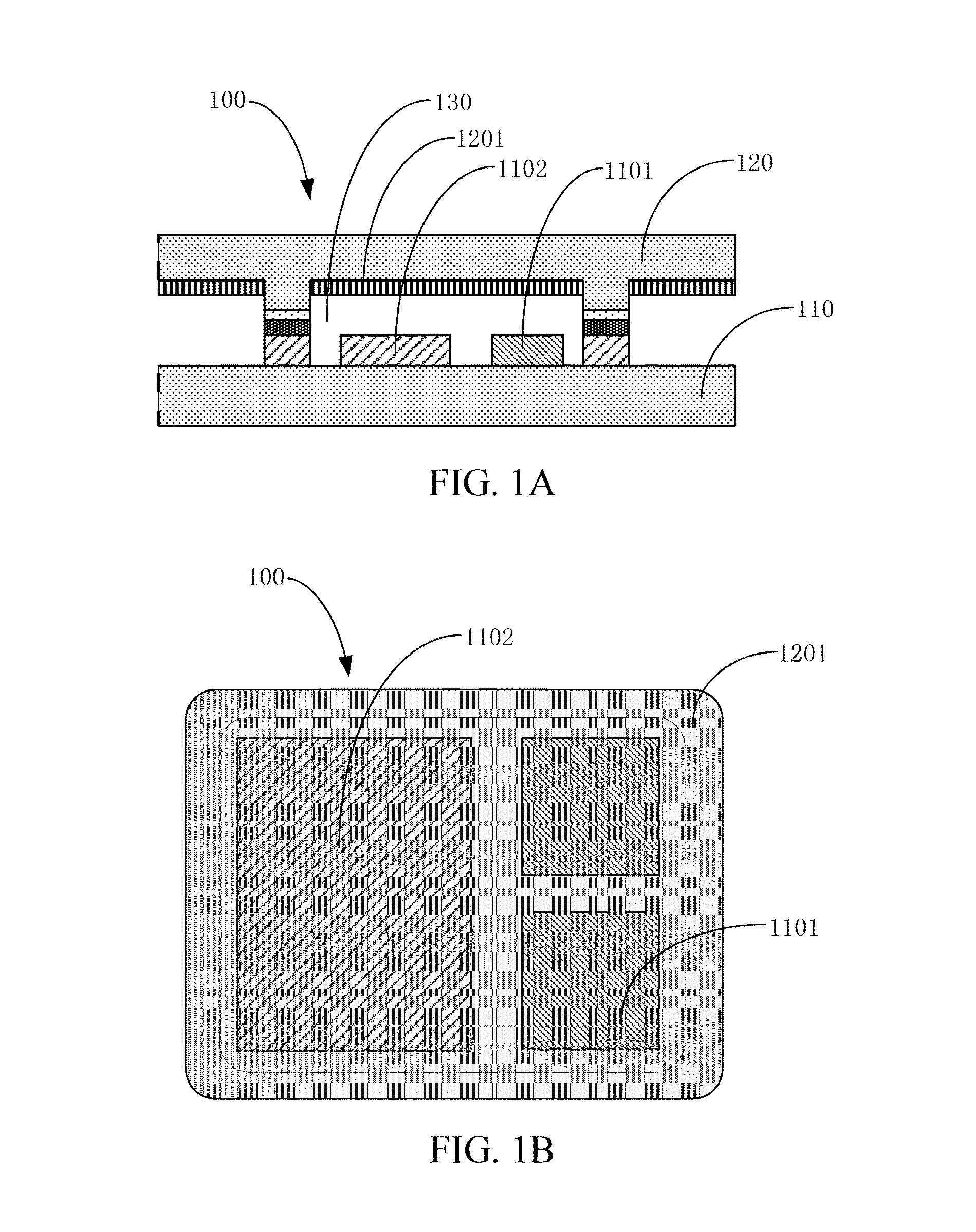
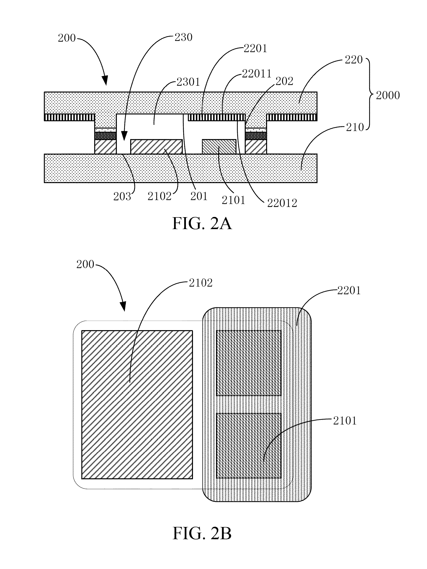
[0034]Example embodiments of the present invention are described with reference to the accompanying drawings. As those skilled in the art would realize, the described embodiments may be modified in various different ways, all without departing from the spirit or scope of the present invention. Embodiments of the present invention may be practiced without some or all of these specific details. Well known process steps and / or structures may not have been described in detail in order to not unnecessarily obscure the present invention.

[0035]The drawings and description are illustrative and not restrictive. Like reference numerals may designate like (e.g., analogous or identical) elements in the specification. Repetition of description may be avoided.

[0036]The relative sizes and thicknesses of elements shown in the drawings are for facilitate description and understanding, without limiting the present invention. In the drawings, the thicknesses of some layers, films, panels, regions, etc...


PUM


Abstract

A semiconductor device may include an enclosure structure. The semiconductor device may further include a getter for absorb gas molecules. The getter may be positioned (and enclosed) inside the enclosure structure and may overlap a first portion of a surface of the enclosure structure. The semiconductor device may further include an inductor. The inductor may be positioned (and enclosed) inside the enclosure structure and may overlap a second portion of the surface of the enclosure structure without overlapping the getter in a direction perpendicular to the first surface of the enclosure structure.

Description

CROSS-REFERENCE TO RELATED APPLICATION[0001]This application claims priority to and benefit of Chinese Patent Application No. 201410370715.6, filed on Jul. 30, 2014; the Chinese Patent Application is incorporated herein by reference in its entirety.BACKGROUND OF THE INVENTION[0002]The present invention is related to a semiconductor device, a method for manufacturing the semiconductor device, and an electronic device that includes the semiconductor device.[0003]A semiconductor device may include elements that need to operate in a vacuum environment. For example, the elements may include one or more microelectromechanical systems (MEMS) components. The semiconductor device may include a substantially vacuum structure for accommodating the elements. In order to maintain the vacuum environment, the substantially vacuum structure may include a getter that may combine with and / or absorb gas molecules that emerge in the vacuum environment.[0004]If the getter is undesirably coupled with ano...

Claims


Application Information

Patent Timeline
Patent Type & Authority Patents(United States)
IPC IPC(8): H01L21/76B81B7/00H01L49/02
CPCB81B7/0038H01L28/10H01L23/04H01L23/26H01L23/5227
Inventor ZHENG, CHAOMA, JUNDEGUO, LIANGLIANGWANG, WEI
Owner SEMICON MFG INT (SHANGHAI) CORP
Why Eureka
Try Eureka