Carbon-chalcogenide variable resistance memory device

a memory device and variable resistance technology, applied in the direction of electrical appliances, etc., can solve the problems of other drawbacks of current devices, difficulty in tuning in the high resistance programming range, etc., and achieve the effect of reducing or eliminating

Active Publication Date: 2015-08-25
BOISE STATE UNIVERSITY
View PDF10 Cites 4 Cited by
  • Summary
  • Abstract
  • Description
  • Claims
  • Application Information

AI Technical Summary

Benefits of technology

The present disclosure introduces a memory device that can change its resistance continuously, which solves or reduces the problems of existing devices.

Problems solved by technology

Variable resistance devices, such as the device disclosed in U.S. Pat. No. 7,304,368, which is hereby incorporated by reference, may be difficult to tune in the high resistance programming range, and preferentially operate in a binary mode between high and low resistances.
Other drawbacks of current devices may also exist.

Method used


Image

  • Carbon-chalcogenide variable resistance memory device
  • Carbon-chalcogenide variable resistance memory device
  • Carbon-chalcogenide variable resistance memory device

Examples


Embodiment Construction

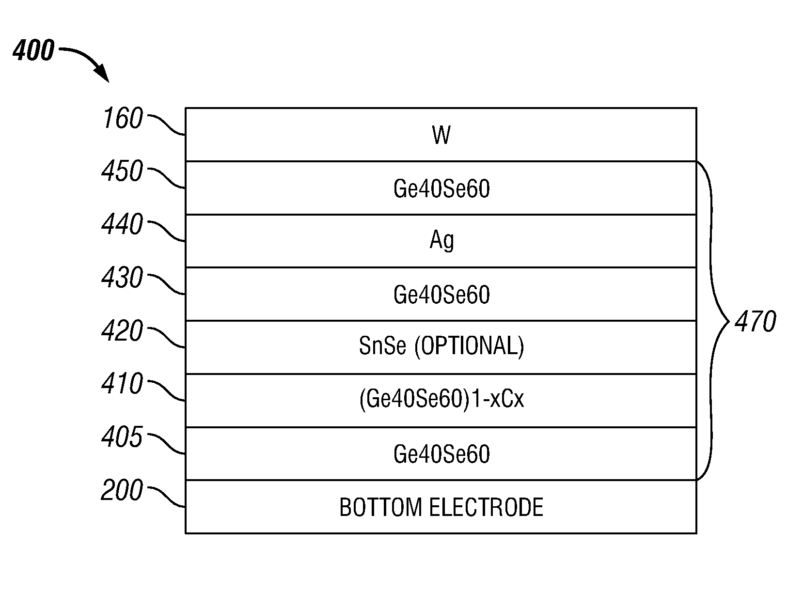
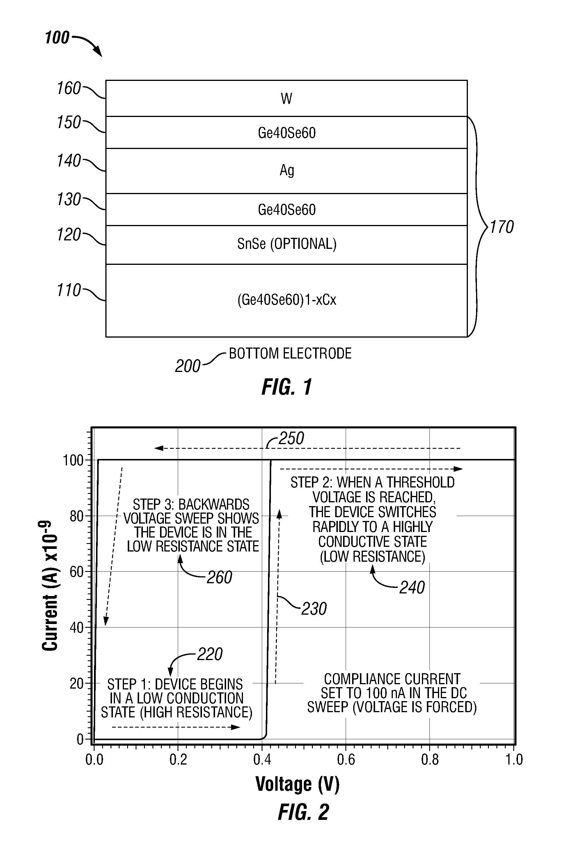
[0026]In the following detailed description, reference is made to various specific embodiments of the application. These embodiments are described with sufficient detail to enable those skilled in the art to practice the invention. It is to be understood that other embodiments may be employed, and that various structural, logical and electrical changes may be made without departing from the spirit or scope of the invention.

[0027]The term “substrate” used in the following description may include any supporting structure including but not limited to a semiconductor substrate that has an exposed substrate surface. A semiconductor substrate should be understood to include silicon-on-insulator (SOI), silicon-on-sapphire (SOS), doped and undoped semiconductors, epitaxial layers of silicon supported by a base semiconductor foundation, and other semiconductor structures. When reference is made to a semiconductor substrate or wafer in the following description, previous process steps may hav...


PUM


Abstract

A variable resistance memory device that includes a first electrode, a second electrode, and a first chalcogenide material layer between the first and second electrodes, the chalcogenide layer including carbon incorporated into germanium selenide chalcogenide glass. The variable resistance memory device may include a second chalcogenide material layer between the first chalcogenide material layer and the second electrode. The variable resistance memory device may include a first metallic layer between the second chalcogenide material layer and the second electrode. The variable resistance memory device may include a third chalcogenide material layer between the first metallic layer and the second electrode. The variable resistance memory device may include a fourth chalcogenide material layer between the first chalcogenide material layer and the first electrode. The first chalcogenide layer may be formed by co-sputtering carbon with Ge40Se60.

Description

FIELD OF THE DISCLOSURE[0001]This disclosure relates generally to continuously variable resistance memory devices, also referred to herein as a memristor. In particular, the disclosure relates to improvements in memristors including, among other things, the ability to program the device to a lower resistance and the ability to tune the device during an erase operation in the higher resistance direction.BACKGROUND[0002]Variable resistance memory devices, also known as resistance variable memory elements, utilizing chalcogenides have been used as semi-volatile and non-volatile random access memory devices. U.S. Pat. No. 6,348,365 entitled “PCRAM Cell Manufacturing” discloses a typical chalcogenide variable resistance memory element. A typical chalcogenide variable resistance memory element often incorporates a conductive material into a chalcogenide glass. The conductive material may typically be silver and / or copper. The resistance of the chalcogenide glass can be “programmed” to hav...

Claims


Application Information

Patent Timeline
IPC IPC(8): H01L45/00
CPCH01L45/143H01L45/1233H01L45/1253H01L45/1625H01L45/149H10N70/245H10N70/8825H10N70/026H10N70/826H10N70/8845
Inventor CAMPBELL, KRISTY A.
Owner BOISE STATE UNIVERSITY
Why Eureka
Try Eureka