Power semiconductor device and method for producing a power semiconductor device

a technology of power semiconductor and semiconductor components, which is applied in semiconductor devices, semiconductor/solid-state device details, cooling/ventilation/heating modifications, etc., can solve the problems of heat loss of power semiconductor components and electrical losses at power semiconductor components, and achieve reliable connection, reliable connection, and reliable connection

Inactive Publication Date: 2015-08-18
SEMIKRON ELECTRONICS GMBH & CO KG
View PDF5 Cites 3 Cited by
  • Summary
  • Abstract
  • Description
  • Claims
  • Application Information

AI Technical Summary

Benefits of technology

[0016]It proves to be advantageous if the first weld seam connects the lateral side surfaces of the cooling plate to lateral side surfaces of the first cooling housing component that delimit the cutout, thereby ensuring a reliable seal of the heat sink.
[0028]Furthermore, it proves to be advantageous if that side surface region of the cooling plate which adjoins the first weld seam and that side surface region of the first cooling housing component which adjoins the first weld seam are arranged flush relative to one another. A particularly reliable and precise connection of the cooling plate to the first cooling housing component is achieved as a result. That side surface region of the cooling plate which adjoins the first weld seam and that side surface region of the first cooling housing component which adjoins the first weld seam preferably run parallel to the insulation layer.

Problems solved by technology

During the operation of the power semiconductor device, electrical losses occur at the power semiconductor components.
These losses heat the power semiconductor components.
However, what is disadvantageous in this case is that the cooling plate has to be sealed in relation to the heat sink reliably and over the long term in order to prevent leakage of the cooling liquid over the service life of the power semiconductor device, which is generally envisaged to last for a long time.

Method used


Image

  • Power semiconductor device and method for producing a power semiconductor device
  • Power semiconductor device and method for producing a power semiconductor device
  • Power semiconductor device and method for producing a power semiconductor device

Examples


Embodiment Construction

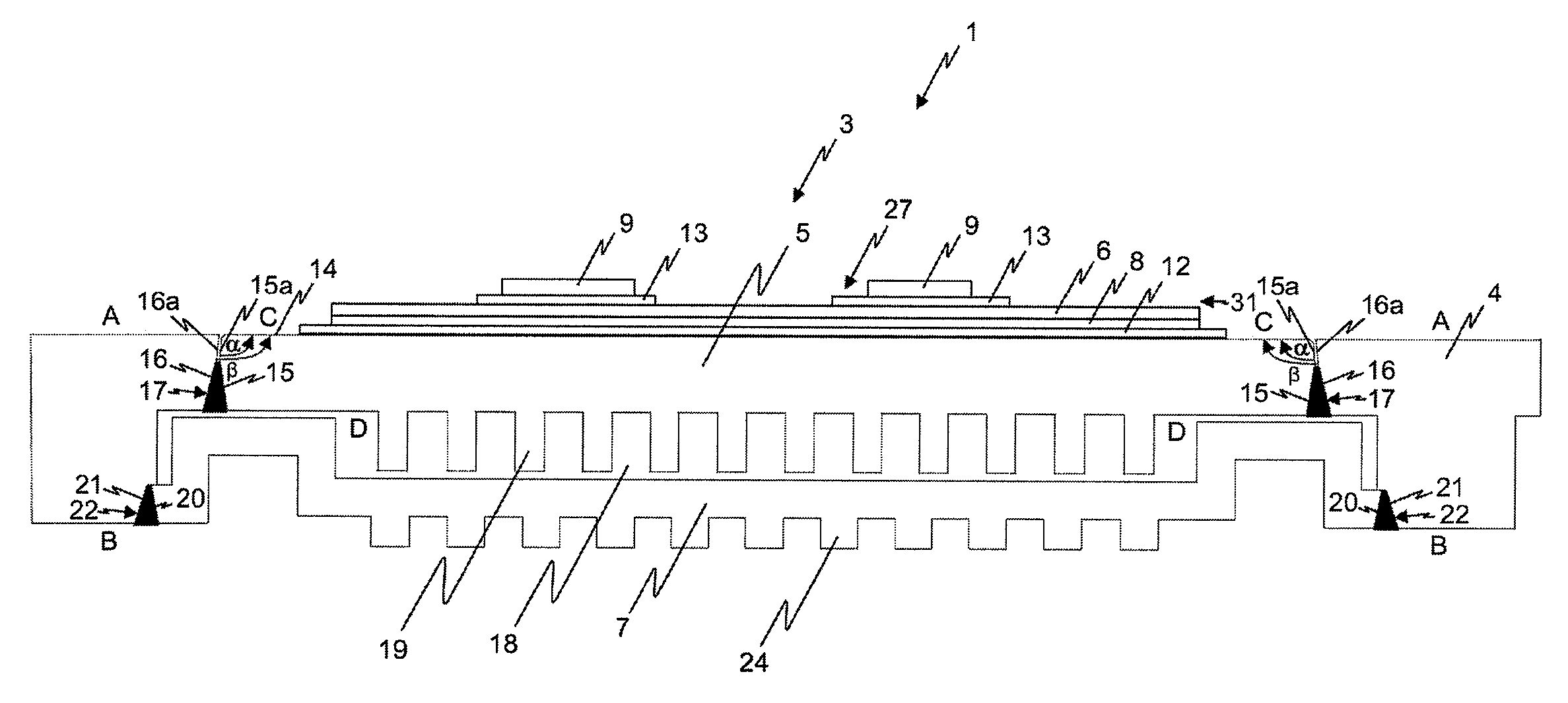
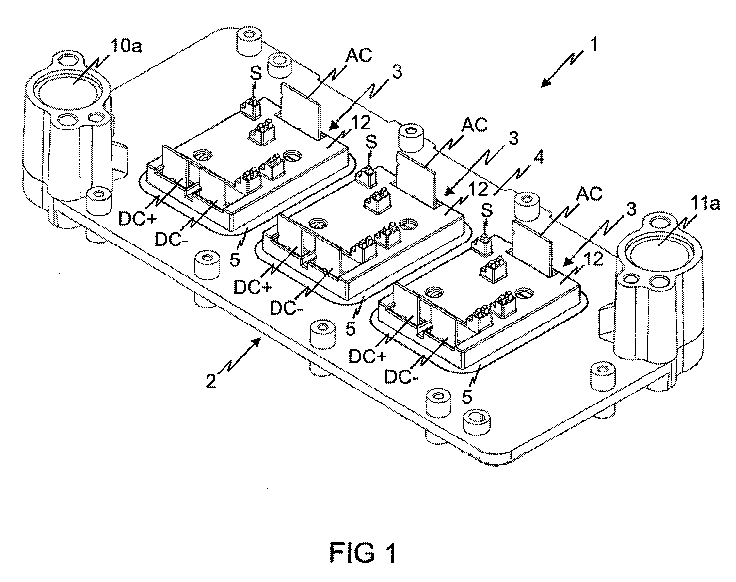
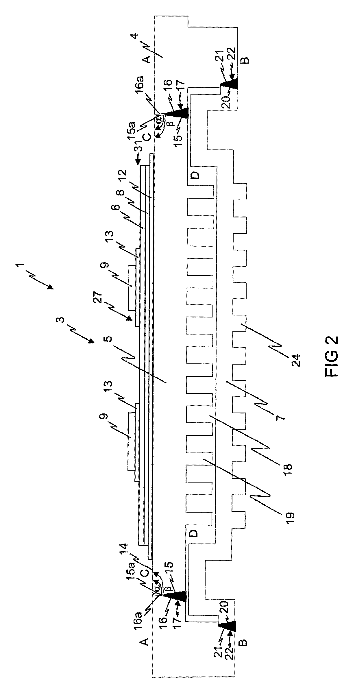
[0042]FIGS. 1, 2 and 4 show a power semiconductor device 1 according to the invention, FIG. 2 and the other sectional views illustrating only those elements of power semiconductor device 1 which are essential for understanding the invention. FIG. 3 illustrates a perspective rear view of a first cooling housing component 4 into which a cooling plate 5 is welded. FIG. 5 illustrates an exploded perspective front view of power semiconductor device 1 in an unassembled state. Power semiconductor device 1 comprises at least one power semiconductor module 3, wherein power semiconductor device 1 can comprise a plurality of individual power semiconductor modules 3 and comprises three such power semiconductor modules 3 in the exemplary embodiment. Each power semiconductor module 3 has at least one power semiconductor component 9 arranged on electrically conductive conductor tracks 13. Conductor tracks 13 are formed by an electrically conductive structured first conduction layer 31. Power semic...


PUM


Abstract

A power semiconductor device comprising a power semiconductor module and a heat sink and a method for its manufacture. The heat sink has a first cooling housing component, with a cutout passing therethrough, and a second cooling housing component, with a cooling plate arranged in the cutout. The first and second cooling housing components are configured and arranged relative to one another so that a cavity is formed at the side of the cooling plate facing away from the power semiconductor components. The cooling plate is connected to the first cooling housing component by a first weld seam which extends circumferentially therearound. The first weld seam seals the cooling plate in relation to the first cooling housing component, and the second cooling housing component is connected to the first cooling housing component. The inventive power semiconductor device has good heat conduction from the power semiconductor components to a heat sink.

Description

BACKGROUND OF THE INVENTION[0001]1. Field of the Invention[0002]The invention relates to a power semiconductor device, and to a method for producing a power semiconductor device.[0003]2. Description of the Related Art[0004]Known power semiconductor devices generally include power semiconductor components, such as, e.g., power semiconductor switches and diodes, which are arranged on a substrate and are electrically conductively connected to one another by a conductor layer of the substrate, and bonding wires and / or a film composite. In such known devices, the power semiconductor switches are generally present in the form of transistors, such as, e.g., IGBTs (Insulated Gate Bipolar Transistors) or MOSFETs (Metal Oxide Semiconductor Field Effect Transistors).[0005]In such devices, the power semiconductor components arranged on the substrate are often electrically interconnected to form one or more so-called half-bridge circuits, which are used, e.g., for rectifying and inverting electr...

Claims


Application Information

Patent Timeline
Patent Type & Authority Patents(United States)
IPC IPC(8): H01L23/34H01L23/00H01L23/367H05K7/20H01L21/48
CPCH01L23/3675H01L21/4882H01L23/3672H01L23/3677H01L24/83H05K7/20927H01L2224/83237H01L2224/83238H01L2224/83801H01L2924/13091H01L2924/20103H01L2924/20104H01L2924/1305H01L2924/13055H01L2924/15747H01L2924/12042H01L2924/00
Inventor BOGEN, INGOBECK, MARKUSKULAS, HARTMUTPOPESCU, ALEXANDERHELLDORFER, REINHARD
Owner SEMIKRON ELECTRONICS GMBH & CO KG
Why Eureka
Try Eureka