Method, device and data structure for data storage on memory devices

a technology of memory devices and data structures, applied in the direction of memory architecture accessing/allocation, memory adressing/allocation/relocation, instruments, etc., can solve the problems of affecting the manufacture time, deteriorating the writing speed experienced by the user, and requiring a large amount of processing, so as to increase the throughput of the manufacture line, increase flexibility, and save time

Active Publication Date: 2015-05-26
META PLATFORMS INC
View PDF11 Cites 0 Cited by
  • Summary
  • Abstract
  • Description
  • Claims
  • Application Information

AI Technical Summary

Benefits of technology

[0022]The method of storing data according to an embodiment of the invention allows creating single data images for programming memory devices having differently sized erasable units. The data structure suggested by this invention enables one or more data units to be combined into a single erasable unit, wherein each data unit has its own data unit header for storing the data unit status information. This information will be valid for all data units in an erase unit. Therefore file system images using this data structure can be used—without any need for changes or re-generation—for memory devices that have erasable units of sizes ranging from the first value up to higher multiples thereof.
[0024]Therefore the invention allows for increased flexibility for the manufacturers of electronic devices comprising memory devices having different erasable unit sizes, because the same file system image (e.g. comprising the embedded software, operating system, pre-programmed content etc.) can be used. If in the same model / type of electronic device (or generally product) another type of memory device shall be used than the one used in the initial production batch, for example due to a change in supplier of the memory devices, this is possible without requiring the generation of a new file system image. This saves time, i.e. increases the throughput of the manufacture line, and offers the manufacturer a much less restrictive choice in the memory devices used in a certain product.

Problems solved by technology

Irrespective of the particular flash file system solution this content needs to be programmed to the non-volatile memory as fast as possible during manufacture such that manufacture time is not increased too much, because the manufacture time affects the price of the product and mass manufacture capabilities.
Naturally this strongly deteriorates the writing speed experienced by the user.
Therefore a conversion is required between an application writing data and the actual physical writing operations, so that a considerable amount of processing is needed.
Thus during manufacture of a product, for example a mobile phone or other electronic device, programming of the embedded software and / or pre-programmed content into the flash memory strongly affects the manufacture time.
Therefore the usage of conventional flash file system approaches as described before is not suitable for mass manufacture from the point of view of manufacture speed.
With the conventional flash file systems the size of the erasable unit has to be known beforehand, thus strongly reducing the flexibility of the manufacturer of an electronic device.
This makes mass manufacture complicated as pre-generated flash images cannot be used because normally a flash file system handles its own functionality based on erasable unit size.
If an individual image is created for each flash type product the software distribution and maintenance get too complex.
Apparently the known flash file systems are disadvantageous for manufacturers of electronic products, because they either reduce the possible choices of memory types for the product or make the manufacture time-consuming and expensive.

Method used


Image

  • Method, device and data structure for data storage on memory devices
  • Method, device and data structure for data storage on memory devices
  • Method, device and data structure for data storage on memory devices

Examples


Embodiment Construction

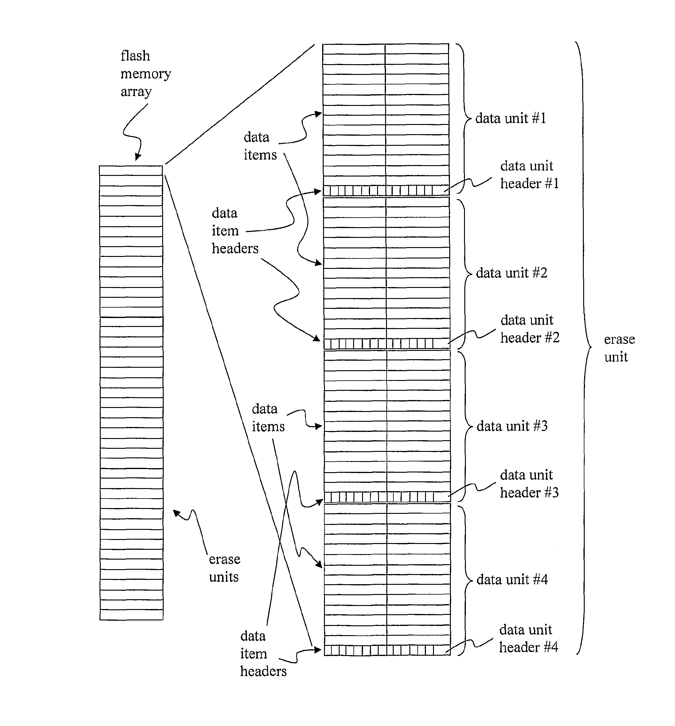
[0048]It is to be noted that the following description will mainly focus on flash memory devices as an example of non-volatile memory devices to which the invention can be applied. However, the invention is not limited to a use with flash memory including but not limited to NOR, NAND, Nitrided Read Only Memory (NROM) and Phase Change memories, but can be used for any non-volatile memory technology that is based on the use of hardware or logical erasable units.

[0049]The invention can be applied to memories that do not have hardware erasable units, but that are implemented with a similar logic functionality. For example due to legacy issues, i.e. backwards compatibility, memories not requiring the use of erasable units may though be logically implemented as if they had erasable units. This means that e.g. the erase functionality and / or the erase commands are used in the same manner as in memories with hardware erasable units. The data structure according to embodiments of the inventio...


PUM


Abstract

A method is provided for storing data on memory devices comprising a plurality of erasable units, wherein the size of said erasable units is an integer multiple of a first integer value, comprising providing a data structure comprising a plurality of data units each including a data unit header, wherein the size of said data units is equal to said first integer value, a plurality of data items and corresponding data item headers within each data unit, associating at least one data unit to each erasable unit, storing said data in said data items and storing data item status information in the corresponding data item headers, and storing data unit status information in said data unit headers.

Description

RELATED APPLICATION[0001]This application was originally filed as PCT Application No. PCT / IB2007 / 004083 filed Dec. 24, 2007.[0002]The present invention relates to methods and devices for storing data on non-volatile memory devices. It also relates to data structures for improving the initial programming of such memory devices during manufacture of electronic devices comprising the non-volatile memory devices.PRIOR ART[0003]Consumer products which have some embedded software usually also include some content for the end user. This content may be music, pictures, applications, end user help notes or even pre-installed settings which help end users using a product. It may also be some data which is used by the product itself. This content and embedded software are usually programmed to a non-volatile memory of the product during manufacture before shipping the product to an end user.[0004]Content is in many cases stored to either a separate memory or to the same non-volatile memory as ...

Claims


Application Information

Patent Timeline
Patent Type & Authority Patents(United States)
IPC IPC(8): G06F12/00G06F13/00G06F13/28G06F9/445G06F12/02G11C16/10
CPCG06F12/0246G06F8/65G06F2212/1004G06F2212/1016G06F2212/7202G06F2212/7206G06F2212/7207G11C16/102
Inventor HANHIMAKI, PETTERIJARVINEN, ILPO HENRIK
Owner META PLATFORMS INC
Why Eureka
Try Eureka