
Integrated voltage divider

a voltage divider and integrated technology, applied in the direction of electrical apparatus contruction details, electrical circuit non-printed electric components association, etc., can solve the problems of not always being available in modern electronic devices, increasing costs and lowering manufacturing yields, and still expensive design

Active Publication Date: 2015-05-26
STMICROELECTRONICS SRL
View PDF5 Cites 0 Cited by
  • Summary
  • Abstract
  • Description
  • Claims
  • Application Information

AI Technical Summary

Benefits of technology

This solution enables compact and cost-effective generation of intermediate voltage levels without additional resistors, improving manufacturing efficiency and reducing board size, while maintaining reliability and flexibility in voltage control.

Problems solved by technology

Such a design is nevertheless expensive since it requires the addition of resistors 6005 and 6006 on the board.
Moreover, the presence of the resistors 6005 and 6006 on the board requires a larger board area, which may not always be available in modern electronic devices.
Furthermore, the presence of resistors 6005 and 6006 on the board requires additional manufacturing steps, thereby also increasing costs and lowering manufacturing yield.

Method used


Image

  • Integrated voltage divider
  • Integrated voltage divider
  • Integrated voltage divider

Examples


Embodiment Construction

[0049]FIG. 4a illustrates a top view of semiconductor structure 4000 contained within first semiconductor chip 6001 of circuit 6000 board of FIG. 6. FIG. 4b illustrates a section of semiconductor structure 4000 of FIG. 4a taken along line A-A′.

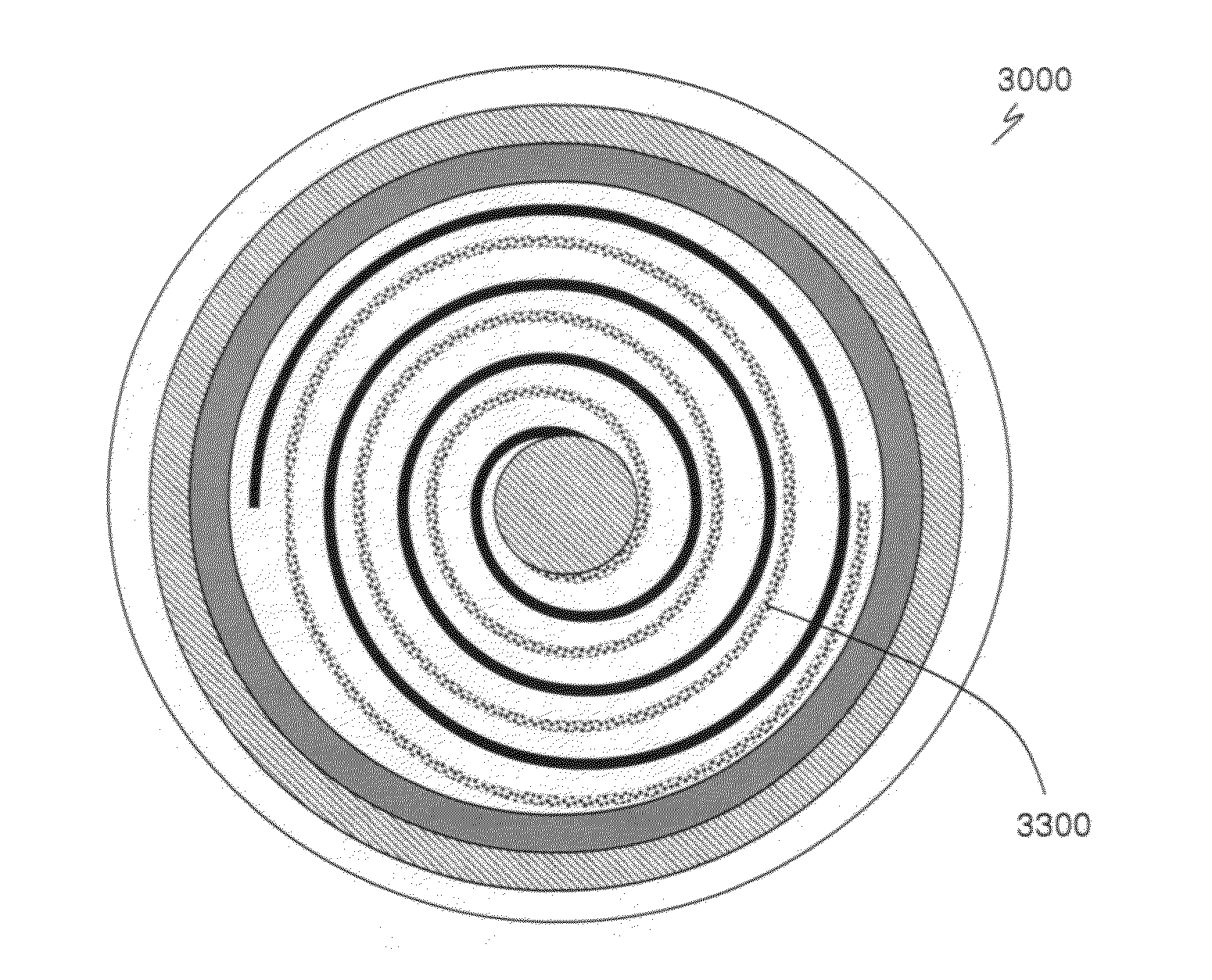
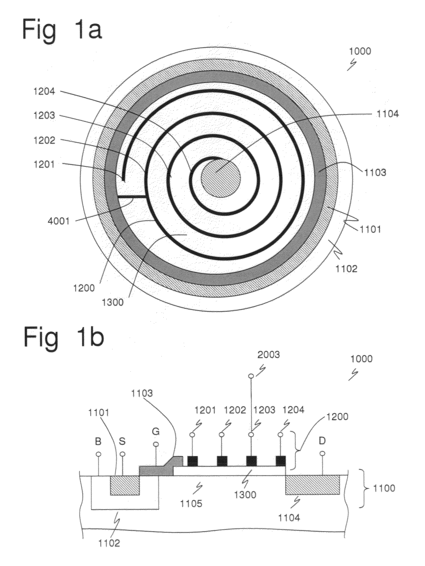
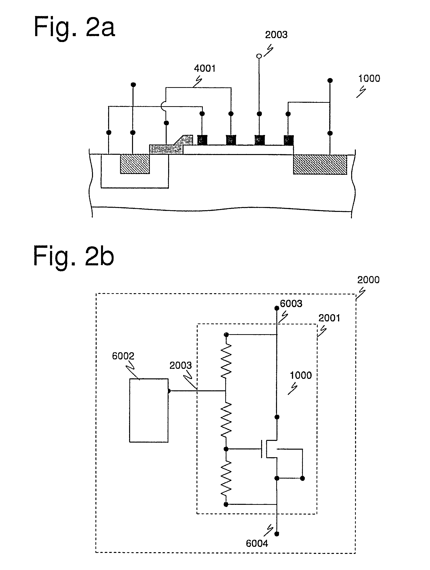
[0050]As can be seen in FIGS. 4a and 4b, semiconductor structure 4000 comprises a high voltage transistor 1100 and voltage dropping element 1200. More specifically, the high voltage transistor 1100 comprises a source 1101, a body 1102, a gate 1103, a drain 1104 and a drift region 1105. In the case, for instance, of an N-MOS high voltage transistor 1100, the drain 1104 is N+ doped, so as the source 1101. At the same time, the body 1102 is P doped while the drift region 1105 is N doped. With such an arrangement, a current can flow from the drain 1104 to the source 1101 depending on the voltage applied to the gate 1103, by using the drift region 1105 as a resistor.

[0051]The dopants for the P doped regions could be any of Boron and / or Indium in a ...


PUM


Abstract

A semiconductor structure including a high-voltage transistor; voltage dropping circuitry, at least part of which is overlapping the high-voltage transistor; at least one intermediate contact point to the voltage dropping circuitry, connected to at least one intermediate position between a first and a second end of the voltage dropping circuitry; and at least one external connection connecting the at least one intermediate contact point to outside of the semiconductor structure.

Description

CROSS REFERENCE TO RELATED APPLICATIONS[0001]This application claims the priority benefit of Italian patent application number VI2011A000247, filed on Sep. 15, 2011, which is hereby incorporated by reference to the maximum extent allowable by law.BACKGROUND[0002]1. Technical Field[0003]The present disclosure relates to a semiconductor structure comprising a high-voltage transistor; voltage dropping means, at least part of which is overlapping the high-voltage transistor; at least one intermediate contact point to the voltage dropping means, connected to at least one intermediate position between a first and a second end of the voltage dropping means.[0004]2. Discussion of the Related Art[0005]In recent years, the requirement for smaller electronic devices has forced manufacturers of such devices to integrate more and more components within printed semiconductor chips.[0006]Additionally, it is common to have high voltages, in the range of 300 to 500 volts, or even higher, on a printe...

Claims


Application Information

Patent Timeline
Patent Type & Authority Patents(United States)
IPC IPC(8): H01L27/06H01K1/18H01L29/78H01L29/861H01L49/02H01L29/06H10N97/00
CPCH01L29/7817H01L29/7818H01L29/861H01L28/20H01L29/0692H01L29/0696
Inventor DEPETRO, RICCARDONOVELLI, ALDO VITTORIOBELLOMO, IGNAZIO SALVATORE
Owner STMICROELECTRONICS SRL
Learn More