
OLEDs comprising light extraction substructures and display devices incorporating the same

a technology of light extraction substructure and display device, which is applied in the direction of thermoelectric device junction material, semiconductor device, electrical apparatus, etc., can solve the problems of 45% trapped in the organic material of the device and approximately 30% trapped in the glass layer of the device, so as to reduce the entrapment within the glass layer, enhance the light extraction effect, and generate efficient

Active Publication Date: 2014-12-09
CORNING INC
View PDF35 Cites 4 Cited by
  • Summary
  • Abstract
  • Description
  • Claims
  • Application Information

AI Technical Summary

Benefits of technology

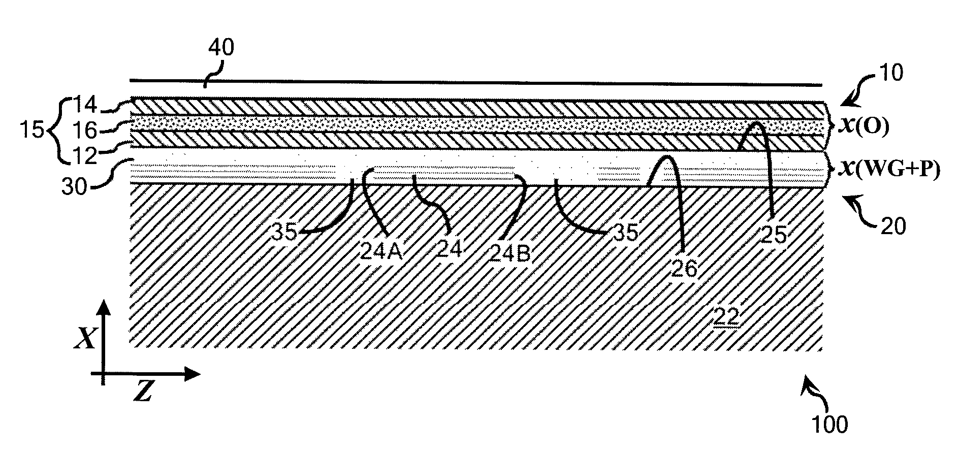
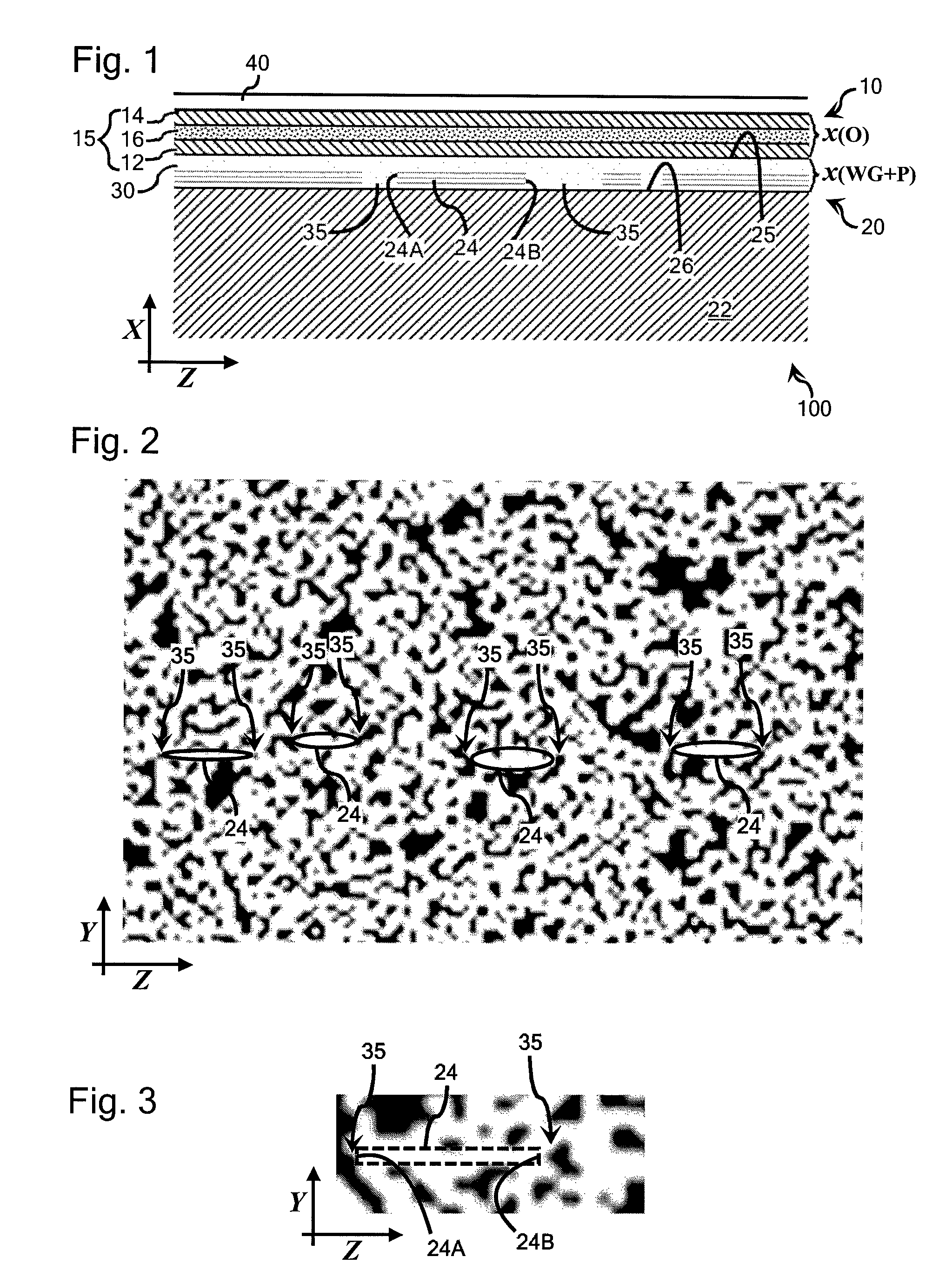
[0004]The present inventors have recognized that, although light can be efficiently generated in OLED devices, much of the generated light remains trapped in the device. In fact, in many devices, only approximately 25% of the generated light escapes to the environment, leaving approximately 45% trapped in the organic material of the device and approximately 30% trapped in the glass layer of the device. According to the subject matter of the present disclosure, a light extraction substructure is provided that enhances light extraction from the organic material of the OLED device and reduces entrapment within the glass layer of the device. The proposed substructure may incorporate chemically strengthened glass such as, for example, ion-exchanged glass. In addition, the glass of the proposed substructure can be manufactured in high volumes using, for example, a fusion draw process.

Problems solved by technology

In fact, in many devices, only approximately 25% of the generated light escapes to the environment, leaving approximately 45% trapped in the organic material of the device and approximately 30% trapped in the glass layer of the device.

Method used


Image

  • OLEDs comprising light extraction substructures and display devices incorporating the same
  • OLEDs comprising light extraction substructures and display devices incorporating the same
  • OLEDs comprising light extraction substructures and display devices incorporating the same

Examples


examples

[0034]FIG. 6 shows intensity obtained for the device (FIG. 6A) fabricated according to the schematic of FIG. 1 but without the smoothing or planarization layer. Left side of the device contains the nanoparticles on the OLED and the right side contains only the OLED. The intensity difference is shown on the graph (FIG. 6B) where the increased intensity (3.4×) in the presence of the scattering sites.

[0035]FIG. 7 shows SEMS of a glass with a scattering layers and planarization layer / s. FIG. 7A shows a ˜2 um thickness total and FIG. 7B shows a 3.7 μm thickness. In both pictures, the scattering layer shows up as the white particles at the lower interface and the planarizing layer is the roughened surface above the scattering layer.

[0036]Table 1 shows AFM RMS roughness measurements for the corresponding SEMS shown in FIG. 7A (˜2 μm thickness) and FIG. 7B (3.7 μm thickness). Total RMS surface roughness shows a dependence on binder depth as well as agglomerate size.

[0037]

TABLE 1Thickness(SE...


PUM


Abstract

An organic light emitting diode comprising a light extraction substructure and a diode superstructure is provided. The light extraction substructure comprises a light expulsion matrix distributed over discrete light extraction waveguide elements and a waveguide surface of the glass substrate. The light expulsion matrix is distributed at varying thicknesses to enhance the planarity of a diode superstructure-engaging side of the light extraction substructure and to provide light expulsion sites at the waveguide element termination points of the discrete light extraction waveguide elements. In operation, light originating in the organic light emitting semiconductor material of the diode superstructure is coupled to the discrete waveguide elements of the light extraction substructure as respective coupled modes characterized by an approximate coupling length defined as the propagation distance required for an optical mode to be coupled from the superstructure waveguide to one of the discrete waveguide elements of the light extraction substructure.

Description

CROSS-REFERENCE TO RELATED APPLICATIONS[0001]This application claims the benefit of priority under 35 U.S.C. §119 of U.S. Provisional Application Ser. No. 61 / 708,196, filed on Oct. 1, 2012, the content of which is relied upon and incorporated herein by reference in its entirety.FIELD[0002]The present disclosure relates to organic light emitting diodes (OLEDs) and display devices incorporating the same. For example, contemplated display devices include, but are not limited to, light sources, image displays, visual indicators, or any other device that utilizes one or more light sources to fulfill its function.BACKGROUND[0003]Organic light emitting diodes (OLEDs) are generally attractive for display applications. A variety of OLED configurations have been proposed to increase the operating efficiency and enhance other performance parameters of OLEDs including, for example, those proposed in U.S. Pat. Nos. 7,834,539, 7,824,541, and 7,432,649 and published U.S. Pre-Grant Publications 201...

Claims


Application Information

Patent Timeline
Patent Type & Authority Patents(United States)
IPC IPC(8): H01L51/56H01L51/52
CPCH01L51/5275H01L51/56H01L51/5268H01L51/5262H01L51/5271H10K50/85H10K50/854H10K50/856H10K50/858H10K71/00
Inventor BAKER, DAVID EUGENENOLAN, DANIEL ALOYSIUSQUESADA, MARK ALEJANDROSENARATNE, WAGEESHA
Owner CORNING INC
Learn More