Array of mutually isolated, geiger-mode, avalanche photodiodes and manufacturing method thereof

a technology of mutual isolation and avalanche, which is applied in the direction of diodes, electrical devices, solid-state devices, etc., can solve the problems of high production cost and inability to enable a high level of component integration, and achieve high-density integration and reduce optical and electrical cross-talk

Active Publication Date: 2014-07-15
STMICROELECTRONICS SRL
View PDF37 Cites 6 Cited by
  • Summary
  • Abstract
  • Description
  • Claims
  • Application Information

AI Technical Summary

Benefits of technology

[0023]An embodiment of the present disclosure includes an array of avalanche photodiodes that e...

Problems solved by technology

This latter solution also has the disadvantage of not enabling a h...

Method used


Image

  • Array of mutually isolated, geiger-mode, avalanche photodiodes and manufacturing method thereof
  • Array of mutually isolated, geiger-mode, avalanche photodiodes and manufacturing method thereof
  • Array of mutually isolated, geiger-mode, avalanche photodiodes and manufacturing method thereof

Examples


Embodiment Construction

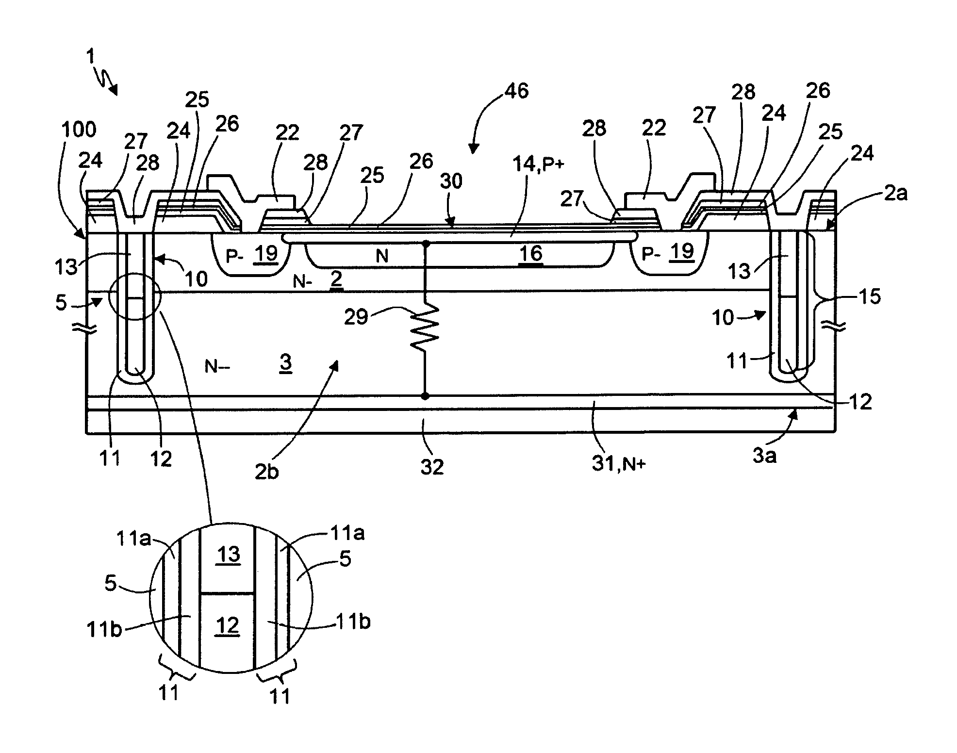
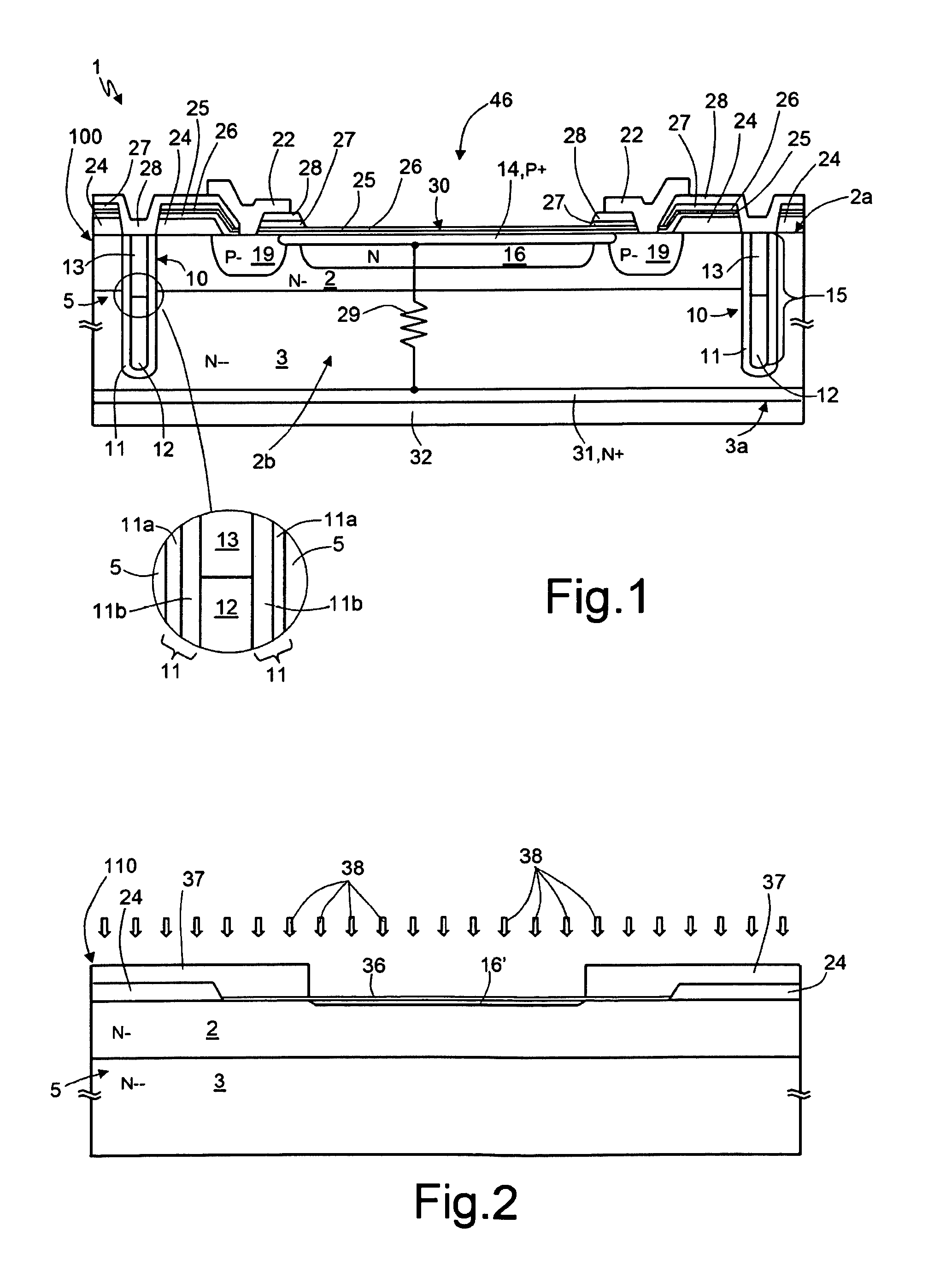
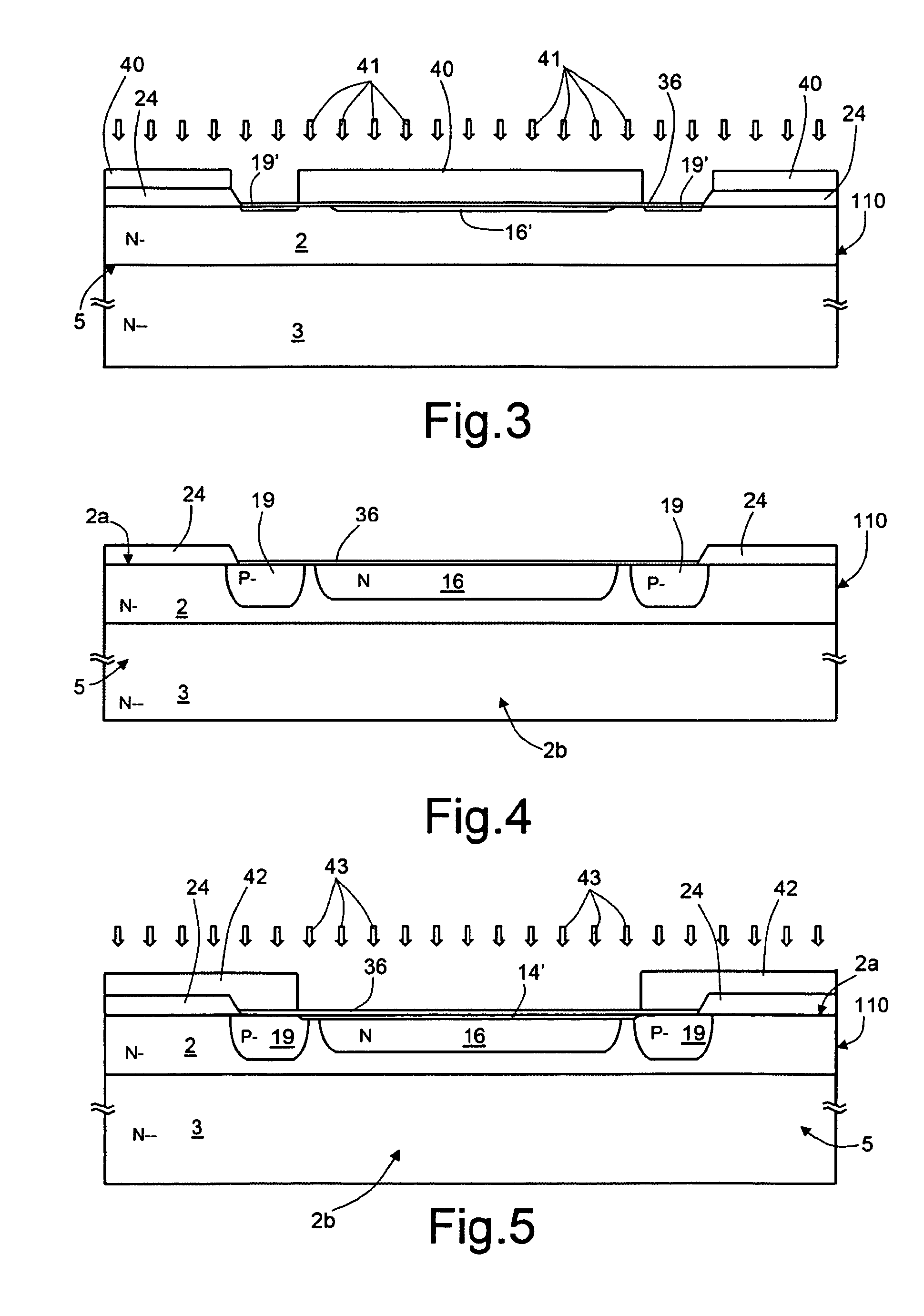
[0034]FIG. 1 shows an embodiment of a photodiode 1 of a Geiger type belonging to an array 220 (shown in FIG. 16) of photodiodes 1. The array 220 may comprise any number of photodiodes 1 according to the application.

[0035]The photodiode 1 is integrated in a chip 100 including an epitaxial layer 2 of an N− type having a top surface 2a and overlying, in direct contact, a substrate 3, of an N−− type, for example, of a float-zone type. The substrate 3 has a bottom surface 3a. The substrate 3 and the epitaxial layer 2 form in practice a body 5 of semiconductor material.

[0036]A substrate of a float-zone type may be characterized by a high purity level for reducing the presence of sites where avalanche carrier generation in dark conditions may occur.

[0037]A deep lateral insulation region 10 having, in top view, a circular or polygonal shape, extends vertically through the epitaxial layer 2 and part of the substrate 3 so as to delimit and insulate portions of the body 5, each forming an acti...


PUM


Abstract

An embodiment of array of Geiger-mode avalanche photodiodes, wherein each photodiode is formed by a body of semiconductor material, having a first conductivity type and housing an anode region, of a second conductivity type, facing a top surface of the body, a cathode-contact region, having the first conductivity type and a higher doping level than the body, facing a bottom surface of the body, an insulation region extending through the body and insulating an active area from the rest of the body, the active area housing the anode region and the cathode-contact region. The insulation region is formed by a first mirror region of polycrystalline silicon, a second mirror region of metal material, and a channel-stopper region of dielectric material, surrounding the first and second mirror regions.

Description

PRIORITY CLAIM[0001]The present application claims the benefit of Italian Patent Application Serial No.: TO2008A000046, filed Jan. 18, 2008, which application is incorporated herein by reference in its entirety.RELATED APPLICATION DATA[0002]This application is related to the U.S. patent application Ser. No. 12 / 356,464, entitled ARRAY OF MUTUALLY INSULATED GEIGER-MODE AVALANCHE PHOTODIODES, AND CORRESPONDING MANUFACTURING PROCESS filed Jan. 20, 2009, now U.S. Pat. No. 8,471,293, Issued Jun. 25, 2013 and which is incorporated herein in its entirety. The present application is also related to U.S. patent application Ser. No. 12 / 637,628, entitled GEIGER-MODE PHOTODIODE WITH INTEGRATED AND ADJUSTABLE QUENCHING RESISTOR, PHOTODIODE ARRAY, AND MANUFACTURING METHOD THEREOF filed Dec. 14, 2009; U.S. patent application Ser. No. 12 / 764,888, entitled GEIGER-MODE PHOTODIODE WITH INTEGRATED AND JFET-EFFECT-ADJUSTABLE QUENCHING RESISTOR, PHOTODIODE ARRAY, AND CORRESPONDING MANUFACTURING METHOD fil...

Claims


Application Information

Patent Timeline
IPC IPC(8): H01L31/0232
CPCH01L31/107H01L27/14643H01L25/167H01L27/14629H01L2924/0002H01L2924/00
Inventor SANFILIPPO, DELFO NUNZIATOFALLICA, PIERO GIORGIO
Owner STMICROELECTRONICS SRL
Why Eureka
Try Eureka