Touch sensor and display device
a display device and touch sensor technology, applied in the field of display devices, can solve the problems of difficult to use liquid crystal display elements for mobile device applications, hardly integrated devices, and hardly detected objects in distant places from touch sensors, so as to improve detection sensitivity and detection sensitivity.
- Summary
- Abstract
- Description
- Claims
- Application Information
AI Technical Summary
Benefits of technology
Problems solved by technology
Method used
Image
Examples
first embodiment
Configuration Example of Display Device 1A
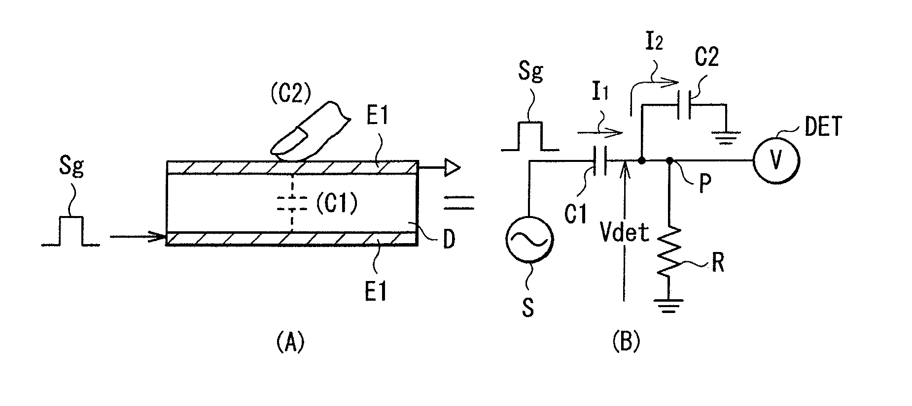
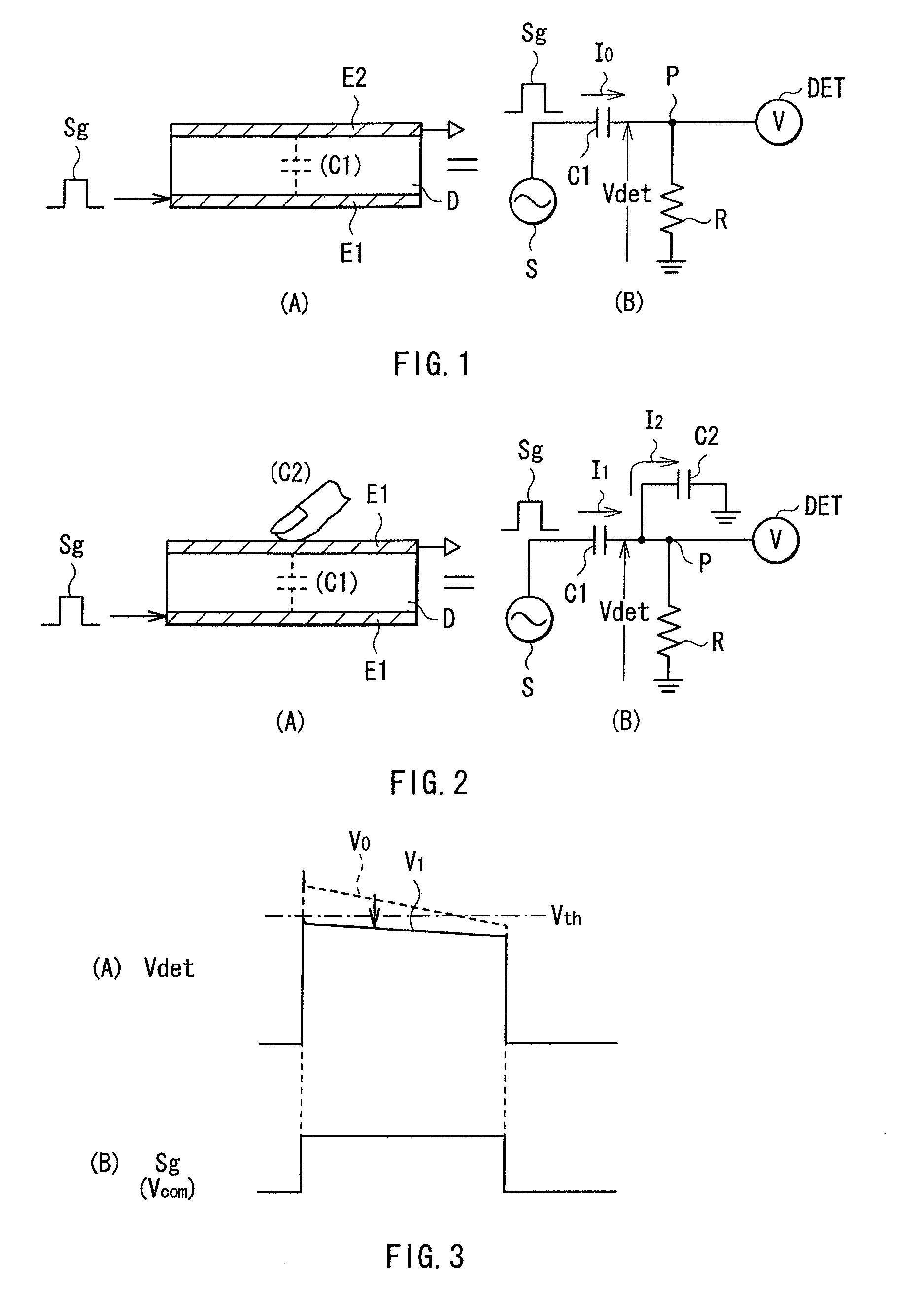
[0065]FIG. 5 shows a relevant-part section structure of a display device 1A according to a first embodiment of the invention. In the display device 1A, a liquid crystal display element is used as a display element, and part of an electrode (a common electrode 43 described later) originally provided in the liquid crystal display element and a display drive signal (common drive signal Vcom described later) are commonly used to configure a capacitance-type touch sensor. The display device 1A includes a pixel substrate 2, a counter substrate 4 disposed facing the pixel substrate 2, and a liquid crystal layer 6 inserted between the pixel substrate 2 and the counter substrate 4.
[0066]The pixel substrate 2 has a TFT substrate 21 as a circuit board, and a plurality of pixel electrodes 22 arranged in a matrix pattern on the TFT substrate 21. On the TFT substrate 21, a not-shown display driver and TFT (Thin Film Transistor) for driving each pixel elec...
second embodiment
Operation and Effects of Second Embodiment
[0116]In the embodiment, while display is performed by the same operation as in the display device 1A of the first embodiment, a detection signal is supplied from the sensor detection electrode 44 to the detection circuit 8 along with scanning the common electrode 43 with a common drive signal Vcom, and thus the detection result Dout is outputted.
Detection Operation in the Embodiment
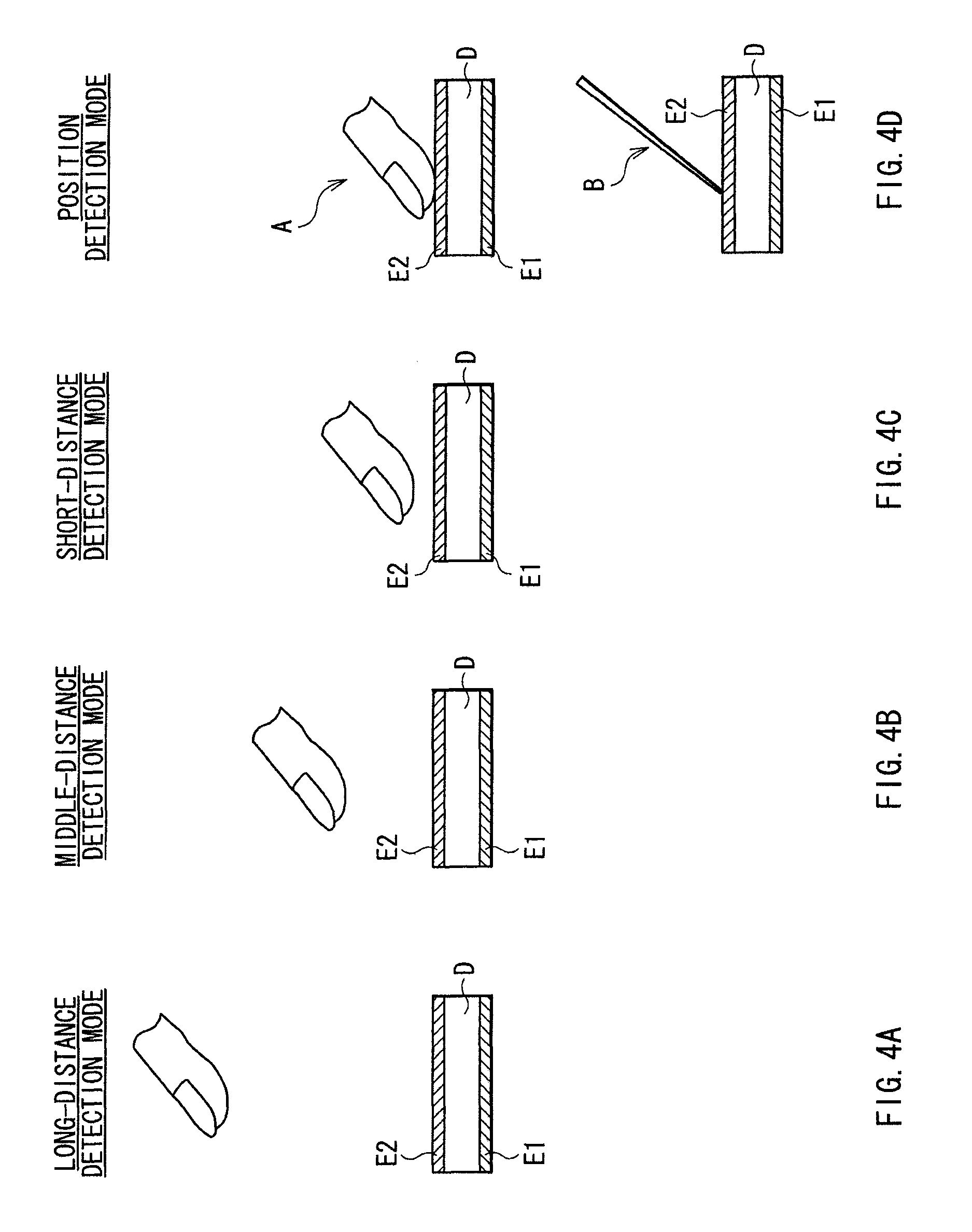
[0117]However, in the embodiment, among all electrode patterns of the sensor detection electrode 44, a selective number of effective electrode patterns is changed in each detection mode. Specifically, in the long-distance detection mode, one detection electrode pattern or a number close to one of the detection electrode patterns (here, two patterns disposed on outermost sides) of all the detection electrode patterns of the sensor detection electrode 44 are selected as effective electrode patterns 44A as shown in FIG. 13A. In contrast, in the position detection mo...
third embodiment
[0129]FIGS. 15A to 15D schematically show inverted waveforms (AC square waves Sg) of a detection drive signal (Vcom2) according to a third embodiment of the invention in each of the detection modes. In the above embodiment, the selective number of the drive electrode patterns in line-sequential drive of the common electrode 43 is changed, or the selective number of the effective electrode patterns of the sensor detection electrode 44 is changed as a measure to change a range of an electric line of force. In the third embodiment, a drive signal Vcom2, which is applied to each drive electrode pattern in line-sequential drive of the common electrode 43, is changed. The embodiment, which is applied to a capacitance-type touch sensor similar to the display device 1A of the first embodiment, is described with, as an example, a case where gradual detection is performed from a long-distance detection mode to a position detection mode. Hereinafter, the same components as in the display devic...
PUM
 Abstract
Description
Claims
Application Information
 - R&D
- Intellectual Property
- Life Sciences
- Materials
- Tech Scout
- Unparalleled Data Quality
- Higher Quality Content
- 60% Fewer Hallucinations
Browse by: Latest US Patents, China's latest patents, Technical Efficacy Thesaurus, Application Domain, Technology Topic, Popular Technical Reports.
© 2025 PatSnap. All rights reserved.Legal|Privacy policy|Modern Slavery Act Transparency Statement|Sitemap|About US| Contact US: help@patsnap.com


