MEMS switch and communication device using the same
a technology of communication device and switch, applied in the field ofmems, can solve the problems of increasing contact resistance, reducing contact area, and not exerting contact force to the entire contact area, and achieves the effects of avoiding the dispersion of contact force, high reliability, and low power
- Summary
- Abstract
- Description
- Claims
- Application Information
AI Technical Summary
Benefits of technology
Problems solved by technology
Method used
Image

Examples
first embodiment
(First Embodiment)
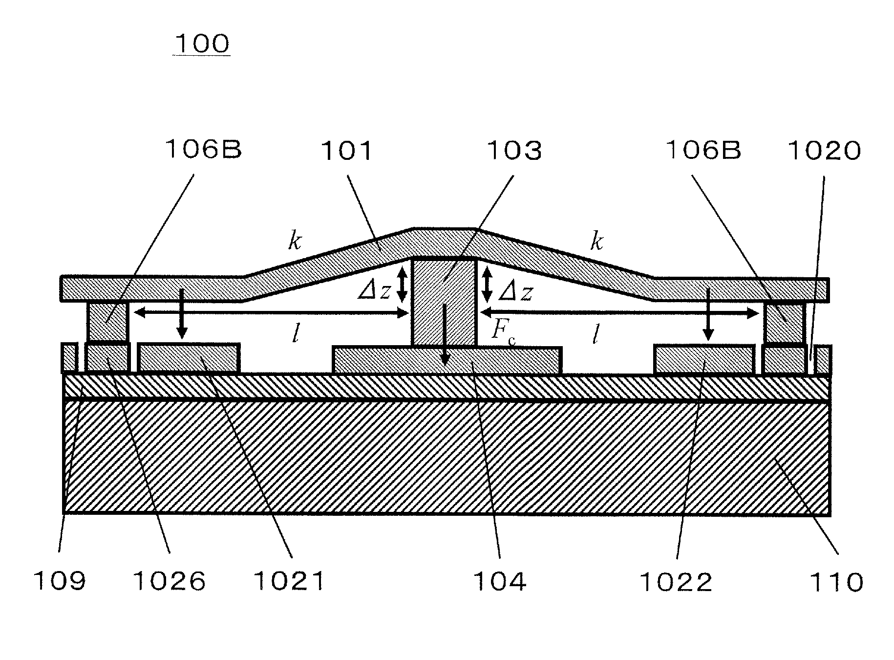
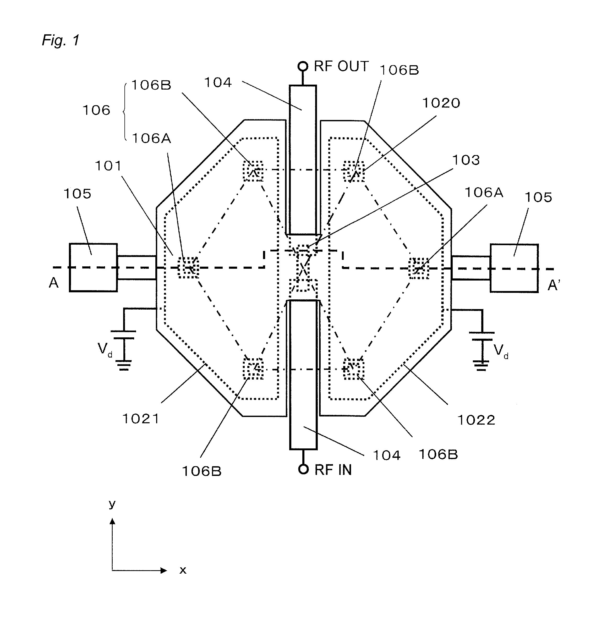
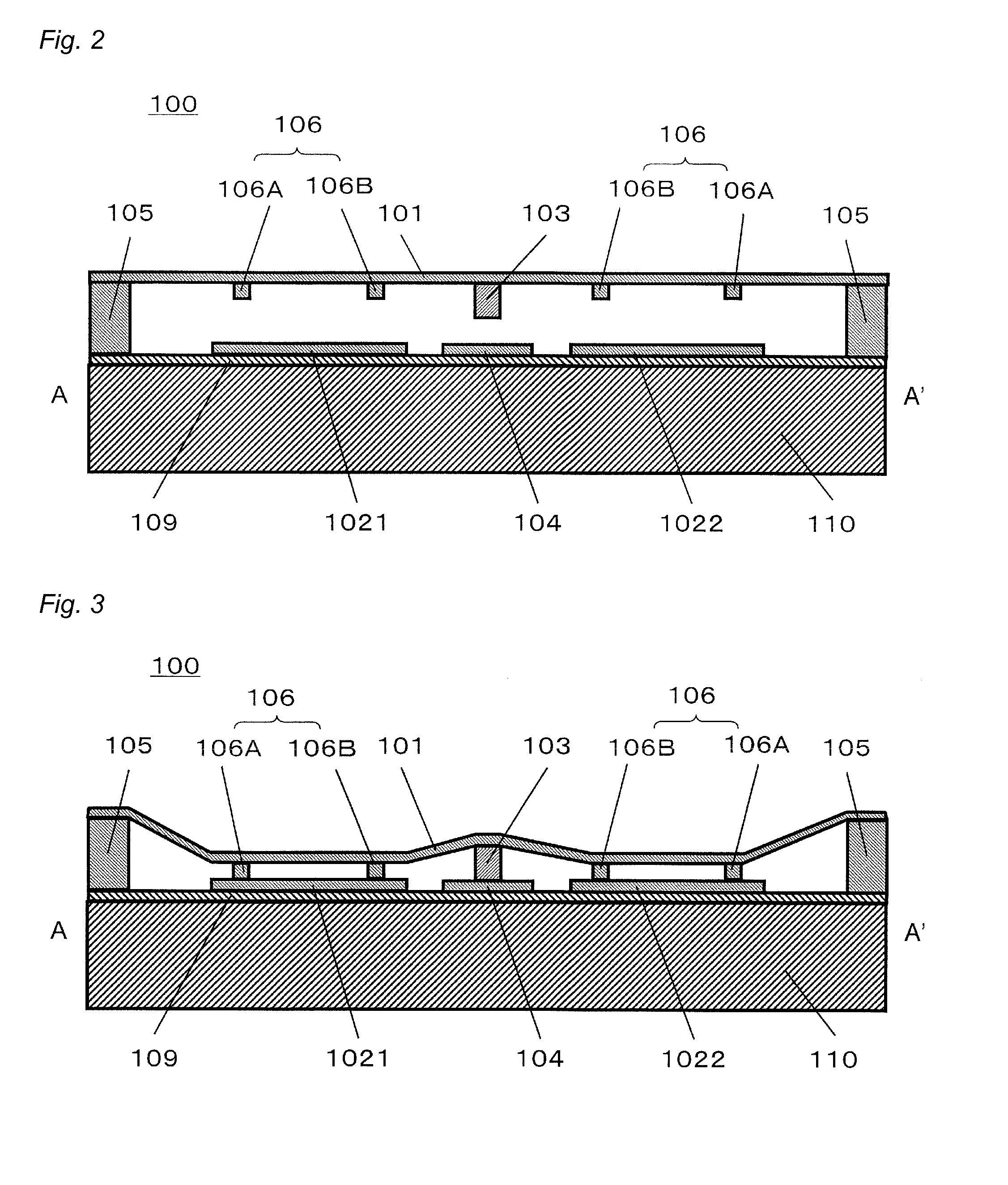
[0042]FIG. 1 is a top view showing a construction of a MEMS switch according to a first embodiment of the present invention. FIG. 2 shows a cross-sectional view along a A-A′ line in FIG. 1 showing a construction of the MEMS element in “off” state. FIG. 3 shows a cross-sectional view along the line A-A′ in FIG. 1 showing a construction of the MEMS switch in “on” state.
[0043]The MEMS switch 100 shown in FIGS. 1 to 3 is a series-type. In this switch, an insulating layer 109 is provided, which is to be an interlayer insulating film, on a substrate 110, and on the insulating layer 109, a driving electrode 1021 as a third electrode, a driving electrode 1022 as a fourth electrode and a signal electrode 104 as a second electrode which becomes a transmission path of a signal are formed. A movable electrode 101 of a fixed-fixed beam type as a first electrode is provided, which is bridged by two supports 105 such that it is opposed to and separated from these electrodes. The ...
second embodiment
(Second Embodiment)
[0069]The embodiment in which the driving electrodes 1021 and 1022 are constructed as the third and the fourth electrodes is described in the first embodiment. The construction in which the driving electrodes are provided on the side of the movable electrode as the first electrode is shown as a second embodiment. FIG. 7 is a cross-sectional view showing the construction of the MEMS switch of the second embodiment. The top view of this MEMS switch is approximately the same as that of the first embodiment (i.e. FIG. 1), and FIG. 7 shows the A-A′ cross section in FIG. 1.
[0070]In the MEMS switch 200 shown in FIG. 7, the insulating layer 109 which is to be an interlayer insulating film 109 is provided on the substrate 110, and two counter electrodes 1121 and 1122 as the third and the fourth electrodes and the signal electrode as the second electrode which is to be the transmission path of the signal are provided on the insulating layer 109. A movable electrode 201 of t...
third embodiment
(Third Embodiment)
[0073]The switches in which the movable electrodes are of fixed-fixed beam type are described in the first and the second embodiments. Now, an embodiment in which the movable electrode is of cantilever type is described as a third embodiment. In the MEMS switch shown in FIG. 8, an insulating layer 309 which is to be the interlayer insulating layer is provided on a substrate 310, and driving electrodes 302 as the third electrode and a signal electrode 304 as the second electrode which is to be the transmission path of signals are formed on the insulating layer 309. A movable electrode 301 having a contact electrode 303 is provided, which is supported by supports 305 such that it is opposed to these electrodes and separated from these electrodes. Bumps 306 (306A, 306B) are provided on the movable electrode 301.
[0074]The mechanism of the switching in the MEMS switch 300 is as described in connection with the first embodiment. Specifically, the voltage is applied to th...
PUM
 Abstract
Description
Claims
Application Information
 - R&D
- Intellectual Property
- Life Sciences
- Materials
- Tech Scout
- Unparalleled Data Quality
- Higher Quality Content
- 60% Fewer Hallucinations
Browse by: Latest US Patents, China's latest patents, Technical Efficacy Thesaurus, Application Domain, Technology Topic, Popular Technical Reports.
© 2025 PatSnap. All rights reserved.Legal|Privacy policy|Modern Slavery Act Transparency Statement|Sitemap|About US| Contact US: help@patsnap.com