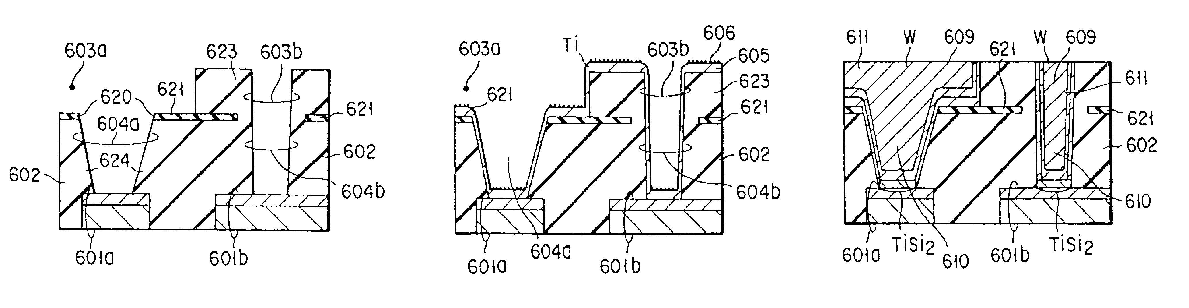
Semiconductor device with tapered contact hole and wire groove
a technology of contact hole and wire groove, which is applied in the direction of semiconductor devices, semiconductor/solid-state device details, electrical apparatus, etc., can solve the problems of reducing yield or reliability, affecting the service life of the contact hole, so as to prevent the short circuit of the wire. , the embedding characteristic of the conductive material is excellen
- Summary
- Abstract
- Description
- Claims
- Application Information
AI Technical Summary
Benefits of technology
Problems solved by technology
Method used
Image

Examples
first embodiment
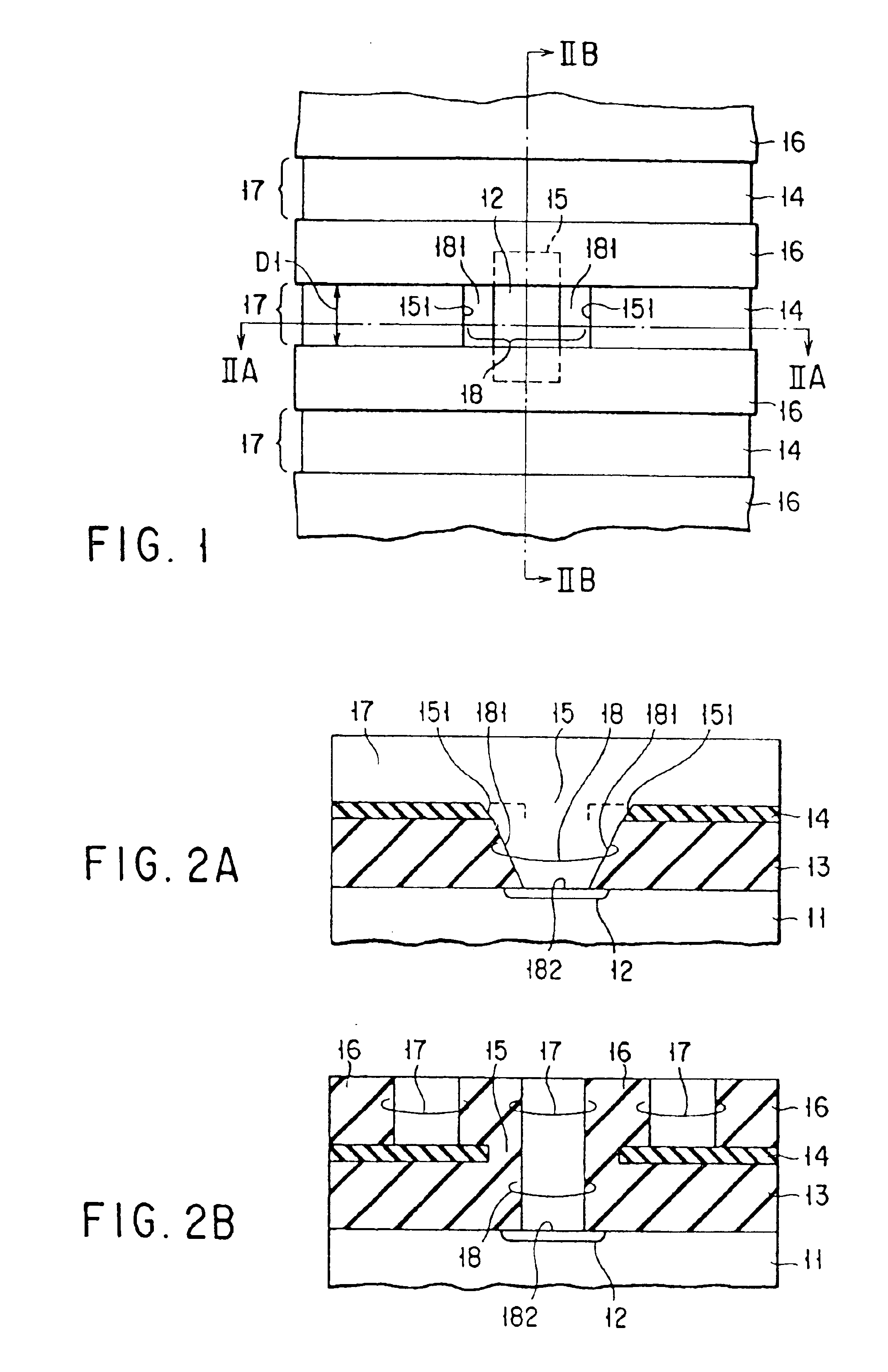
[0073]FIG. 1 is a top plan view showing a wiring groove and a contact hole according to a semiconductor device of the present invention. FIG. 2A and FIG. 2B are sectional views along the lines IIA—IIA and IIB—IIB respectively in FIG. 1.
[0074]In FIGS. 1, 2A and 2B, a first insulation film 13 is formed on a semiconductor substrate 11 including a conductive region 12. The conductive region 12 is a diffused layer, a metal wiring layer or the like. A thin second insulation film 14 which differs in etching rate from the insulation film 13 is deposited on the first insulation film 13. This insulation film 14 is formed with an opening portion 15.
[0075]A third insulation film 16 which differs in etching rate from the insulation film 14 is formed on the first insulation film 13 and second insulation film 14 which are exposed by the opening portion 15. The third insulation film 16 may be formed of the same material as used for the first insulation film 13, specifically, these films may have th...
second embodiment
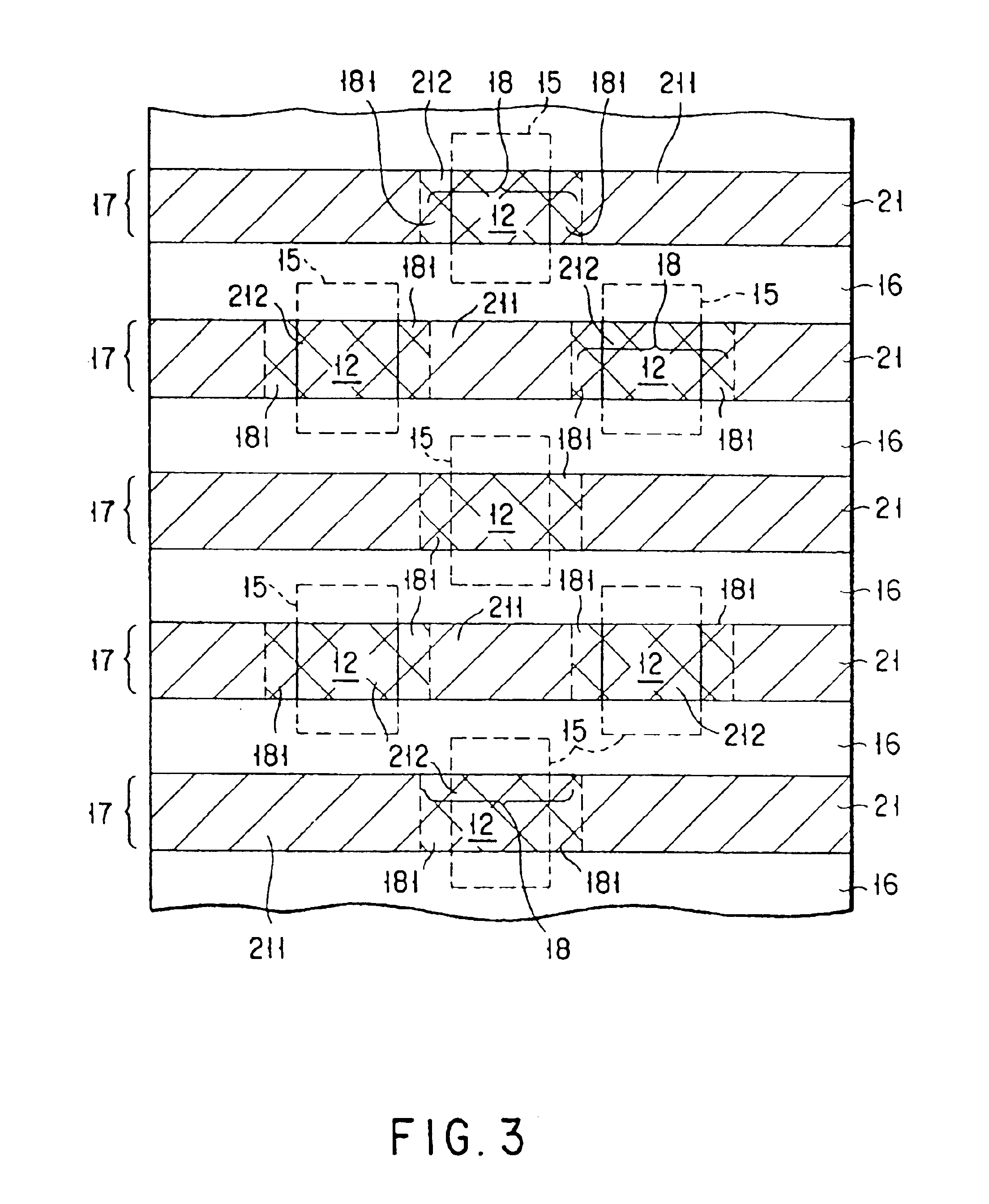
[0094]FIG. 3 is a top plan view showing a contact structure self-aligned with conductive layer embedded in a wiring groove according to a semiconductor device of the present invention. The same parts as in FIG. 1 are represented by the same symbols and explanations of these parts will be omitted.
[0095]An upper layer wiring 211 defined by plural wiring grooves 17 and plural contact plugs 212 connected to the wiring 211 and to an underlying conductive region are formed. These contact plugs 212 are formed along the plural wirings 211, with contact plugs formed along neighboring wirings alternating with each other. Each of the opening portions 15 formed in advance in the second insulation film 14 corresponding to each position of the contact plugs 212 has a rectangular form having a longer side in the direction crossing the wiring groove 17. Each of the opening portions 15 has a shape close to a cross after the contact hole 18 is formed.
[0096]Since the side wall of the wiring groove 17 ...
third embodiment
[0105]FIG. 4 is a top plan view showing a contact structure self-aligned with a conductive layer embedded in a wiring groove according to a semiconductor device of the present invention. The same parts as in FIG. 1 are represented by the same symbols and explanations of these parts will be omitted.
[0106]An upper layer wiring 211 defined by plural wiring grooves 17 and plural contact plugs 212 to which the wiring 211 and an underlying conductive region are connected are formed. These contact plugs 212 are formed along the plural wirings 211, with each corresponding contact plug being arranged in the same position on each wiring 211. Each of the opening portions 15a formed in advance in the second insulation film 14 corresponding to the position of the contact plug 212 has a slit form crossing plural wiring grooves 17. After each contact hole 18 is formed, each slit opening portion 15a exhibits a configuration with an etched recess portion crossing the slit along the wiring groove 17....
PUM
 Abstract
Description
Claims
Application Information
 - R&D
- Intellectual Property
- Life Sciences
- Materials
- Tech Scout
- Unparalleled Data Quality
- Higher Quality Content
- 60% Fewer Hallucinations
Browse by: Latest US Patents, China's latest patents, Technical Efficacy Thesaurus, Application Domain, Technology Topic, Popular Technical Reports.
© 2025 PatSnap. All rights reserved.Legal|Privacy policy|Modern Slavery Act Transparency Statement|Sitemap|About US| Contact US: help@patsnap.com